Absolute maximum ratings, Electrical characteristics – Rainbow Electronics MAX1499 User Manual
Page 2
MAX1497/MAX1499
3.5- and 4.5-Digit, Single-Chip ADCs with LED
Drivers and µC Interface
2
_______________________________________________________________________________________
ABSOLUTE MAXIMUM RATINGS
Stresses beyond those listed under “Absolute Maximum Ratings” may cause permanent damage to the device. These are stress ratings only, and functional
operation of the device at these or any other conditions beyond those indicated in the operational sections of the specifications is not implied. Exposure to
absolute maximum rating conditions for extended periods may affect device reliability.
AV
DD
to GND (MAX1499).........................................-0.3V to +6V
DV
DD
to GND (MAX1499) ........................................-0.3V to +6V
AIN+, AIN- to GND (MAX1499) ...........VNEG to (AV
DD
to +0.3V)
REF+, REF- to GND (MAX1499) ......... VNEG to (AV
DD
to +0.3V)
LOWBATT to GND (MAX1499) ................-0.3V to (AV
DD
+ 0.3V)
CLK,
EOC, CS, DIN, SCLK,
DOUT to GND (MAX1499) .......................-0.3V to (DV
DD
+ 0.3V)
VNEG to GND (MAX1499) .......................-2.6V to (AV
DD
+ 0.3V)
LED_EN to GND (MAX1499)....................-0.3V to (DV
DD
+ 0.3V)
ISET to GND (MAX1499)..........................-0.3V to (AV
DD
+ 0.3V)
V
DD
to GND (MAX1497) ...........................................-0.3V to +6V
AIN+, AIN- to GND (MAX1497)..............VNEG to (V
DD
to +0.3V)
REF+, REF- to GND (MAX1497) ........... VNEG to (V
DD
to +0.3V)
CLK, EOC, CS, DIN, SCLK,
DOUT to GND (MAX1497)..........................-0.3V to (V
DD
+ 0.3V)
VNEG to GND (MAX1497)..........................-2.6V to (V
DD
+ 0.3V)
ISET to GND (MAX1497) ............................-0.3V to (V
DD
+ 0.3V)
VLED to GLED ..........................................................-0.3V to +6V
GLED to GND ........................................................-0.3V to +0.3V
SEG_ to GLED..........................................-0.3V to (VLED + 0.3V)
DIG_ to GLED ..........................................-0.3V to (VLED + 0.3V)
DIG_ Sink Current .............................................................300mA
DIG_ Source Current...........................................................50mA
SEG_ Sink Current ..............................................................50mA
SEG_ Source Current..........................................................50mA
Maximum Current Input into Any Other Pin ........................50mA
Continuous Power Dissipation (T
A
= +70°C)
32-Pin TQFP (derate 20.7mW/°C above +70°C).....1652.9mW
28-Pin SSOP (derate 9.5mW/°C above +70°C) ...........762mW
28-Pin PDIP (derate 14.3mW/°C above +70°C)......1142.9mW
Operating Temperature Range ...........................-40°C to +85°C
Junction Temperature ......................................................+150°C
Storage Temperature Range .............................-60°C to +150°C
Lead Temperature (soldering, 10s) .................................+300°C
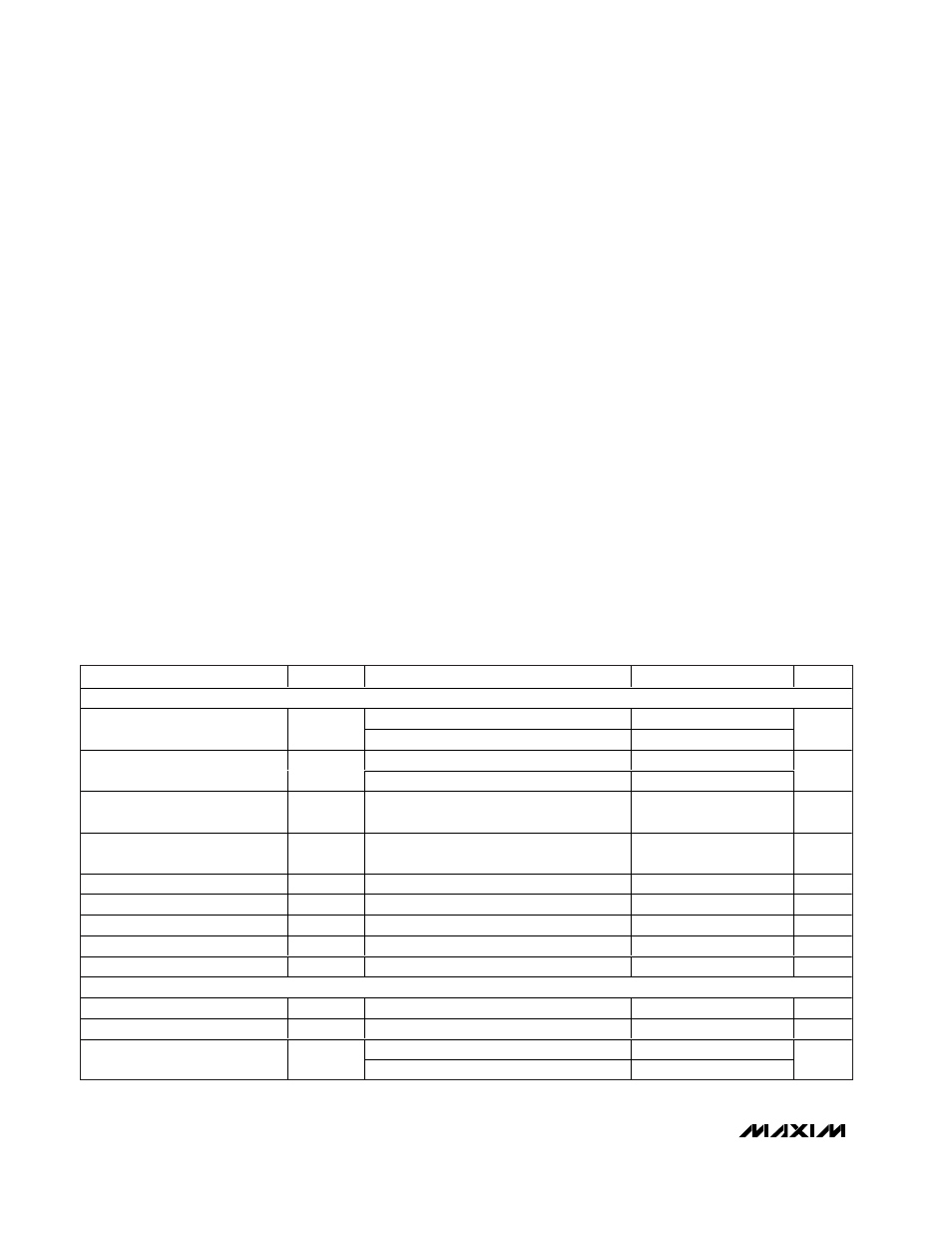
ELECTRICAL CHARACTERISTICS
(AV
DD
= DV
DD
= V
DD
= +2.7V to +5.25V, GND = 0, GLED = 0, V
LED
= +2.7V to +5.25V, V
REF+
- V
REF-
= 2.048V (external reference)
C
REF+
= C
REF-
= 0.1µF, C
VNEG
= 0.1µF. Internal clock mode, unless otherwise noted. All specifications are at T
A
= T
MIN
to T
MAX
.
Typical values are at T
A
= +25°C, unless otherwise noted.)
PARAMETER
SYMBOL
CONDITIONS
MIN
TYP
MAX
UNITS
DC ACCURACY
MAX1499
-19,999
+19,999
Noise-Free Resolution
MAX1497
-1999
+1999
Count
2.000V range
±1
Integral Nonlinearity (Note 1)
INL
200mV range
±1
Count
Range Change Ratio
(V
AIN+
- V
AIN-
= 0.100V) on 200mV range
(V
AIN+
- V
AIN-
= 0.100V) on 2.0V range
10:1
Ratio
Rollover Error
V
AIN+
- V
AIN-
= full scale
V
AIN-
- V
AIN+
= full scale
±1
Count
Output Noise
10
µV
P-P
Offset Error (Zero Input Reading)
Offset
V
IN
= 0 (Note 2)
-0
0
Reading
Gain Error
(Note 3)
-0.5
+0.5
%FSR
Offset Drift (Zero Reading Drift)
V
IN
= 0 (Note 4)
0.1
µV/°C
Gain Drift
±1
ppm/°C
INPUT CONVERSION RATE
External-Clock Frequency
4.9152
MHz
External-Clock Duty Cycle
40
60
%
Internal clock
5
Conversion Rate
External clock, f
CLK
= 4.9152MHz
5
Hz