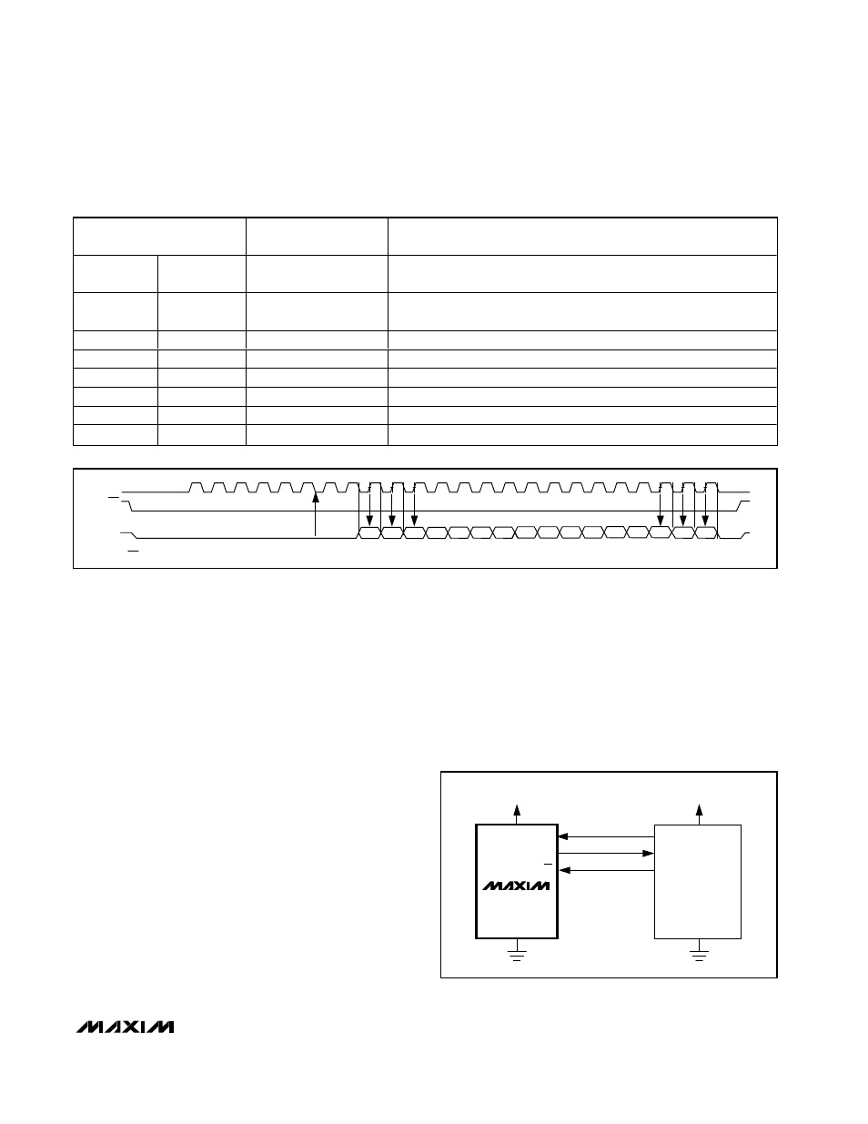
Table 8. detailed sspstat register contents – Rainbow Electronics MAX1168 User Manual
Page 25

MAX1167/MAX1168
Multichannel, 16-Bit, 200ksps Analog-to-Digital
Converters
______________________________________________________________________________________
25
Digital Noise
Digital noise can couple to AIN_ and REF. The conversion
clock (SCLK) and other digital signals active during input
acquisition contribute noise to the conversion result.
Noise signals, synchronous with the sampling interval,
result in an effective input offset. Asynchronous signals
produce random noise on the input, whose high-frequen-
cy components can be aliased into the frequency band
of interest. Minimize noise by presenting a low imped-
ance (at the frequencies contained in the noise signal) at
the inputs. This requires bypassing AIN_ to AGND, or
buffering the input with an amplifier that has a small-sig-
nal bandwidth of several megahertz (doing both is prefer-
able). AIN has a typical bandwidth of 4MHz.
Distortion
Avoid degrading dynamic performance by choosing an
amplifier with distortion much less than the total har-
monic distortion of the MAX1167/MAX1168 at the fre-
quencies of interest (THD = -100dB at 1kHz). If the
chosen amplifier has insufficient common-mode rejec-
tion, which results in degraded THD performance, use
the inverting configuration (positive input grounded) to
eliminate errors from this source. Low-temperature-
coefficient, gain-setting resistors reduce linearity errors
caused by resistance changes due to self-heating. To
reduce linearity errors due to finite amplifier gain, use
amplifier circuits with sufficient loop gain at the fre-
quencies of interest.
DC Accuracy
To improve DC accuracy, choose a buffer with an offset
much less than the MAX1167/MAX1168s’ offset (±10mV
max for +5V supply), or whose offset can be trimmed
while maintaining stability over the required temperature
range.
DOUT*
CS
SCLK
*WHEN CS IS HIGH, DOUT = HIGH-Z
MSB
20
16
D15
D14
D13
D12
D11
D10
D9
HIGH-Z
D1
D0
24
12
1
4
8
6
D8
D5
D4
D3
LSB
D7
D6
SAMPLING INSTANT
D2
Figure 21b. QSPI Interface Timing Sequence (External Clock, 8-Bit Data Transfer, CPOL = CPHA = 0)
CONTROL BIT
SETTINGS
SYNCHRONOUS SERIAL-PORT STATUS REGISTER (SSPSTAT)
SMP
BIT7
0
SPI Data-Input Sample Phase. Input data is sampled at the middle of
the data output time.
CKE
BIT6
1
SPI Clock Edge-Select Bit. Data is transmitted on the rising edge of the
serial clock.
D/A
BIT5
X
Data Address Bit
P
BIT4
X
Stop Bit
S
BIT3
X
Start Bit
R/W
BIT2
X
Read/Write Bit Information
UA
BIT1
X
Update Address
BF
BIT0
X
Buffer-Full Status Bit
Table 8. Detailed SSPSTAT Register Contents
X = Don’t care.
SCK
SDI
GND
PIC16/17
I/O
SCLK
DOUT
CS
V
DD
V
DD
MAX1167
MAX1168
Figure 22a. SPI-Interface Connection for a PIC16/PIC17
