Detailed description, Pin description (continued), Analog input – Rainbow Electronics MAX1168 User Manual
Page 11

Detailed Description
The MAX1167/MAX1168 low-power, multichannel, 16-bit
ADCs feature a successive-approximation ADC, auto-
matic power-down, integrated +4.096V reference, and a
high-speed SPI/QSPI/MICROWIRE-compatible interface.
A DSPR input and DSPX output allow the MAX1168 to
communicate with digital signal processors (DSPs) with
no external glue logic. The MAX1167/MAX1168 operate
with a single +5V analog supply and feature a separate
digital supply, allowing direct interfacing with +2.7V to
+5.5V digital logic.
Figures 3 and 4 show the functional diagrams of the
MAX1167/MAX1168, and Figures 5 and 6 show the
MAX1167/MAX1168 in a typical operating circuit. The
serial interface simplifies communication with micro-
processors (µPs).
In external reference mode, the MAX1167/MAX1168
have two power modes: normal mode and shutdown
mode. Driving CS high places the MAX1167/MAX1168 in
shutdown mode, reducing the supply current to 0.6µA
(typ). Pull CS low to place the MAX1167/MAX1168 in
normal operating mode. The internal reference mode
offers software-programmable, power-down options as
shown in Table 5.
In SPI/QSPI/MICROWIRE mode, a falling edge on CS
wakes the analog circuitry and allows SCLK to clock in
data. Acquisition and conversion are initiated by SCLK.
The conversion result is available at DOUT in unipolar
serial format. DOUT is held low until data becomes
available (MSB first) on the 8th falling edge of SCLK
when in 8-bit transfer mode, and on the 16th falling
edge when in 16-bit transfer mode (see the Operating
Modes section). Figure 8 shows the detailed SPI/QSPI/
MICROWIRE serial-interface timing diagram.
In external clock mode, the MAX1168 also interfaces
with DSPs. In DSP mode, a frame-sync pulse from the
DSP initiates a conversion that is driven by SCLK. The
MAX1168 formats a frame-sync pulse to notify the DSP
that the conversion results are available at DOUT in
MSB-first, unipolar, serial-data format. Figure 16 shows
the detailed DSP serial-interface timing diagram (see the
Operating Modes section).
Analog Input
Figure 7 illustrates the input-sampling architecture of
the ADC. The voltage applied at REF or the internal
+4.096V reference sets the full-scale input voltage.
MAX1167/MAX1168
Multichannel, 16-Bit, 200ksps Analog-to-Digital
Converters
______________________________________________________________________________________
11
Pin Description (continued)
PIN
MAX1167
MAX1168
NAME
FUNCTION
—
13
AIN6
Analog Input 6
—
14
AIN7
Analog Input 7
—
23
DSPX
DSP Frame-Sync Transmit Output. A frame-sync pulse at DSPX notifies the DSP that the
MSB data is available at DOUT. Leave DSPX unconnected when not in DSP mode.
—
24
N.C.
No Connection. Not internally connected.
DGND
1mA
C
LOAD
= 30pF
DOUT
DOUT
C
LOAD
= 30pF
1mA
DGND
DV
DD
a) V
OL
TO V
OH
b) HIGH-Z TO V
OL
AND V
OH
TO V
OL
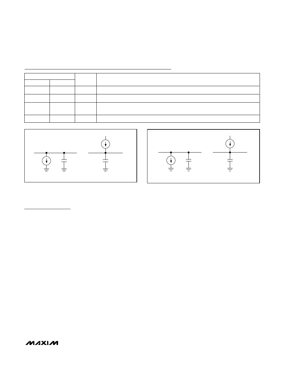
Figure 1. Load Circuits for DOUT Enable Time and SCLK-to-
DOUT Delay Time
DGND
1mA
C
LOAD
= 30pF
DOUT
DOUT
C
LOAD
= 30pF
1mA
DGND
DV
DD
a) V
OH
TO HIGH-Z
b) V
OL
TO HIGH-Z
Figure 2. Load Circuits for DOUT Disable Time
