Rainbow Electronics MAX1168 User Manual
Page 16

MAX1167/MAX1168
Power-Down Modes
Table 5 shows the MAX1167/MAX1168 power-down
modes. Three internal reference modes and one exter-
nal reference mode are available. Select power-down
modes by writing to bits 2 and 1 in the command/con-
figuration/control register. The MAX1167/MAX1168
enter the selected power-down mode on the rising
edge of CS.
The internal reference stays on when CS is pulled high,
if bits 2 and 1 are set to zero. This mode allows for the
fastest turn-on time.
Setting bit 2 = 0 and bit 1 = 1 turns both the reference
and reference buffer off when CS is brought high. This
mode achieves the lowest supply current. The refer-
ence and buffer wake up on the falling edge of CS
when in SPI/QSPI/MICROWIRE mode and on the falling
edge of DSPR when in DSP mode. Allow 5ms for the
internal reference to rise and settle when powering up
from a complete shutdown (V
REF
= 0, C
REF
= 1µF).
The internal reference stays on and the buffer is shut off
on the rising edge of CS when bit 2 = 1 and bit 1 = 0.
The MAX1167/MAX1168 enter this mode on the rising
edge of CS. The buffer wakes up on the falling edge of
CS when in SPI/QSPI/MICROWIRE mode and on the ris-
ing edge of DSPR when in DSP mode. Allow 5ms for
V
REF
to settle when powering up from a complete shut-
down (V
REF
= 0, C
REF
= 1µF). V
REFCAP
is always equal
to +4.096V in this mode.
Set both bit 2 and bit 1 to 1 to turn off the reference and
reference buffer to allow connection of an external ref-
erence. Using an external reference requires no extra
wake-up time.
Operating Modes
External Clock 8-Bit-Wide Data-Transfer Mode
(MAX1167 and MAX1168)
Force DSPR high and DSEL low (MAX1168) for SPI/
QSPI/MICROWIRE interface mode. The falling edge of
CS wakes the analog circuitry and allows SCLK to clock
in data. Ensure the duty cycle on SCLK is between 45%
and 55% when operating at 4.8MHz (the maximum
clock frequency). For lower clock frequencies, ensure
the minimum high and low times are at least 93ns.
External-clock-mode conversions with SCLK rates less
Multichannel, 16-Bit, 200ksps Analog-to-Digital
Converters
16
______________________________________________________________________________________
CS
SCLK
DIN
DOUT
t
CSW
t
CSS
t
CL
t
DS
t
DH
t
DV
t
CH
t
DO
t
TR
t
CSH
t
CP
• • •
• • •
• • •
• • •
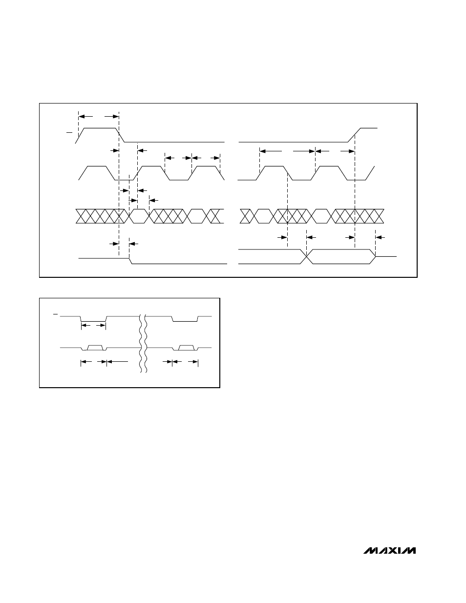
Figure 8. Detailed SPI Interface Timing
COMPLETE CONVERSION SEQUENCE
CONVERSION 0
CONVERSION 1
POWERED UP
POWERED UP POWERED DOWN
DOUT
CS
Figure 9. Shutdown Sequence
