Rainbow Electronics MAX1168 User Manual
Page 17

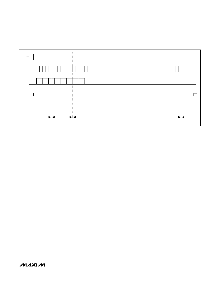
than 125kHz can reduce accuracy due to leakage of the
sampling capacitor. DOUT changes from high-Z to logic
low after CS is brought low. Input data latches on the
rising edge of SCLK. The first SCLK rising edge begins
loading data into the command/configuration/control
register from DIN. The devices select the proper chan-
nel for conversion on the rising edge of the 3rd SCLK
cycle. Acquisition begins immediately thereafter and
ends on the falling edge of the 6th clock cycle. The
MAX1167/MAX1168 sample the input and begin conver-
sion on the falling edge of the 6th clock cycle. Setup
and configuration of the MAX1167/MAX1168 complete
on the rising edge of the 8th clock cycle. The conver-
sion result is available (MSB first) at DOUT on the falling
edge of the 8th SCLK cycle. To read the entire conver-
sion result, 16 SCLK cycles are needed. Extra clock
pulses, occurring after the conversion result has been
clocked out and prior to the rising edge of CS, cause
zeros to be clocked out of DOUT. The MAX1167/
MAX1168 external clock 8-bit-wide data-transfer mode
requires 24 SCLK cycles for completion (Figure 10).
Force CS high after the conversion result is read. For
maximum throughput, force CS low again to initiate the
next conversion immediately after the specified mini-
mum time (t
CSW
). Forcing CS high in the middle of a
conversion immediately aborts the conversion and
places the MAX1167/MAX1168 in shutdown.
External Clock 16-Bit-Wide Data-Transfer Mode
(MAX1168 Only)
Force DSPR high and DSEL high for SPI/QSPI/
MICROWIRE interface mode. Logic high at DSEL allows
the MAX1168 to transfer data in 16-bit-wide words. The
acquisition time is extended an extra eight SCLK cycles
in the 16-bit-wide data-transfer mode. The falling edge of
CS wakes the analog circuitry and allows SCLK to clock
in data. Ensure the duty cycle on SCLK is between 45%
and 55% when operating at 4.8MHz (the maximum clock
frequency). For lower clock frequencies, ensure that the
minimum high and low times are at least 93ns. External-
clock-mode conversions with SCLK rates less than
125kHz can reduce accuracy due to leakage of the sam-
pling capacitor. DOUT changes from high-Z to logic low
after CS is brought low. Input data latches on the rising
edge of SCLK. The first SCLK rising edge begins loading
data into the command/configuration/control register from
DIN. The devices select the proper channel for conver-
sion and begin acquisition on the rising edge of the 3rd
SCLK cycle. Setup and configuration of the MAX1168
completes on the rising edge of the 8th clock cycle.
Acquisition ends on the falling edge of the 14th SCLK
cycle. The MAX1168 samples the input and begins con-
version on the falling edge of the 14th clock cycle. The
conversion result is available (MSB first) at DOUT on the
falling edge of the 16th SCLK cycle. To read the entire
conversion result, 16 SCLK cycles are needed. Extra
clock pulses, occurring after the conversion result has
been clocked out and prior to the rising edge of CS,
cause zeros to be clocked out of DOUT.
MAX1167/MAX1168
Multichannel, 16-Bit, 200ksps Analog-to-Digital
Converters
______________________________________________________________________________________________________
17
DOUT
CS
SCLK
DIN
DSPR*
*MAX1168 ONLY
0
MSB
LSB
MSB
LSB
t
ACQ
IDLE
t
CONV
ADC
STATE
1
8
16
DSEL*
24
Figure 10. SPI External Clock Mode, 8-Bit Data-Transfer Mode, Conversion Timing
