Rainbow Electronics MAX1168 User Manual
Page 18
MAX1167/MAX1168
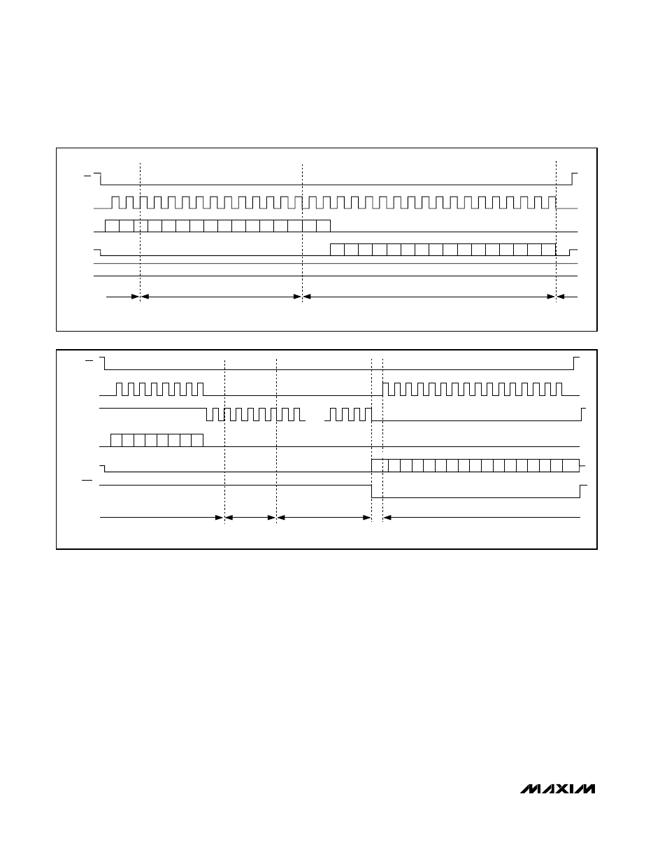
The MAX1168 external clock 16-bit-wide data-transfer
mode requires 32 SCLK cycles for completion (Figure 11).
Force CS high after the conversion result is read. For
maximum throughput, force CS low again to initiate the
next conversion immediately after the specified mini-
mum time (t
CSW
). Forcing CS high in the middle of a
conversion immediately aborts the conversion and
places the MAX1168 in shutdown.
Internal Clock 8-Bit-Wide Data-Transfer and
Scan Mode (MAX1167 and MAX1168)
Force DSPR high and DSEL low (MAX1168) for the SPI/
QSPI/MICROWIRE interface mode. The falling edge of
CS wakes the analog circuitry and allows SCLK to clock
in data (Figure 12). DOUT changes from high-Z to logic
low after CS is brought low. Input data latches on the ris-
ing edge of SCLK. The command/configuration/control
register begins reading DIN on the first SCLK rising edge
and ends on the rising edge of the 8th SCLK cycle. The
MAX1167/MAX1168 select the proper channel for con-
version on the rising edge of the 3rd SCLK cycle. The
internal oscillator activates 125ns after the rising edge of
the 8th SCLK cycle. Turn off the external clock while the
internal clock is on. Turning off SCLK ensures the lowest
noise performance during acquisition. Acquisition begins
on the 2nd rising edge of the internal clock and ends on
the falling edge of the 6th internal clock cycle. Each bit
of the conversion result shifts into memory as it becomes
available. The conversion result is available (MSB first) at
DOUT on the falling edge of EOC. The internal oscillator
and analog circuitry are shut down on the high-to-low
EOC transition. Use the EOC high-to-low transition as the
signal to restart the external clock (SCLK). To read the
Multichannel, 16-Bit, 200ksps Analog-to-Digital
Converters
18
______________________________________________________________________________________
DOUT
CS
SCLK
DIN
DSPR
0
MSB
LSB
MSB
LSB
ADC
STATE
16
24
32
1
8
X
X
X
X
X
X
X
X
X = DON
,
T CARE
t
ACQ
IDLE
t
CONV
DSEL
Figure 11. SPI External Clock Mode, 16-Bit Data-Transfer Mode, Conversion Timing (MAX1168 Only)
DOUT
CS
SCLK
DIN
EOC
1
MSB
LSB
LSB
X
t
ACQ
IDLE
t
CONV
POWER-DOWN
ADC
STATE
X = DON
,
T CARE
DSPR = DV
DD
, DSEL = GND (MAX1168 ONLY)
INTERNAL
CLK
1
8
2
6
25
16
9
24
• • •
MSB
Figure 12. SPI Internal Clock Mode, 8-Bit Data-Transfer Mode, Conversion Timing