Rainbow Electronics MAX1168 User Manual
Page 12
MAX1167/MAX1168
Track/Hold (T/H)
In track mode, the analog signal is acquired on the
internal hold capacitor. In hold mode, the T/H switches
open and the capacitive digital-to-analog converter
(DAC) samples the analog input.
During the acquisition, the analog input (AIN_) charges
capacitor C
DAC
. At the end of the acquisition interval
the T/H switches open. The retained charge on C
DAC
represents a sample of the input.
In hold mode, the capacitive DAC adjusts during the
remainder of the conversion cycle to restore node
ZERO to zero within the limits of 16-bit resolution. At the
end of the conversion, force CS high and then low to
reset the T/H switches back to track mode (AIN_),
where C
DAC
charges to the input signal again.
The time required for the T/H to acquire an input signal
is a function of how quickly its input capacitance is
charged. If the input signal’s source impedance is high,
the acquisition time lengthens and more time must be
allowed between conversions. The acquisition time
(t
ACQ
) is the maximum time the device takes to acquire
the signal. Use the following formula to calculate acqui-
sition time:
t
ACQ
= 11(R
S
+ R
IN
+ R
DS(ON)
)
✕
45pF + 0.3µs
where R
IN
= 340
Ω, R
S
= the input signal’s source
impedance, R
DS(ON)
= 60
Ω, and t
ACQ
is never less
than 729ns. A source impedance of less than 200
Ω
does not significantly affect the ADC’s performance.
Multichannel, 16-Bit, 200ksps Analog-to-Digital
Converters
12
______________________________________________________________________________________
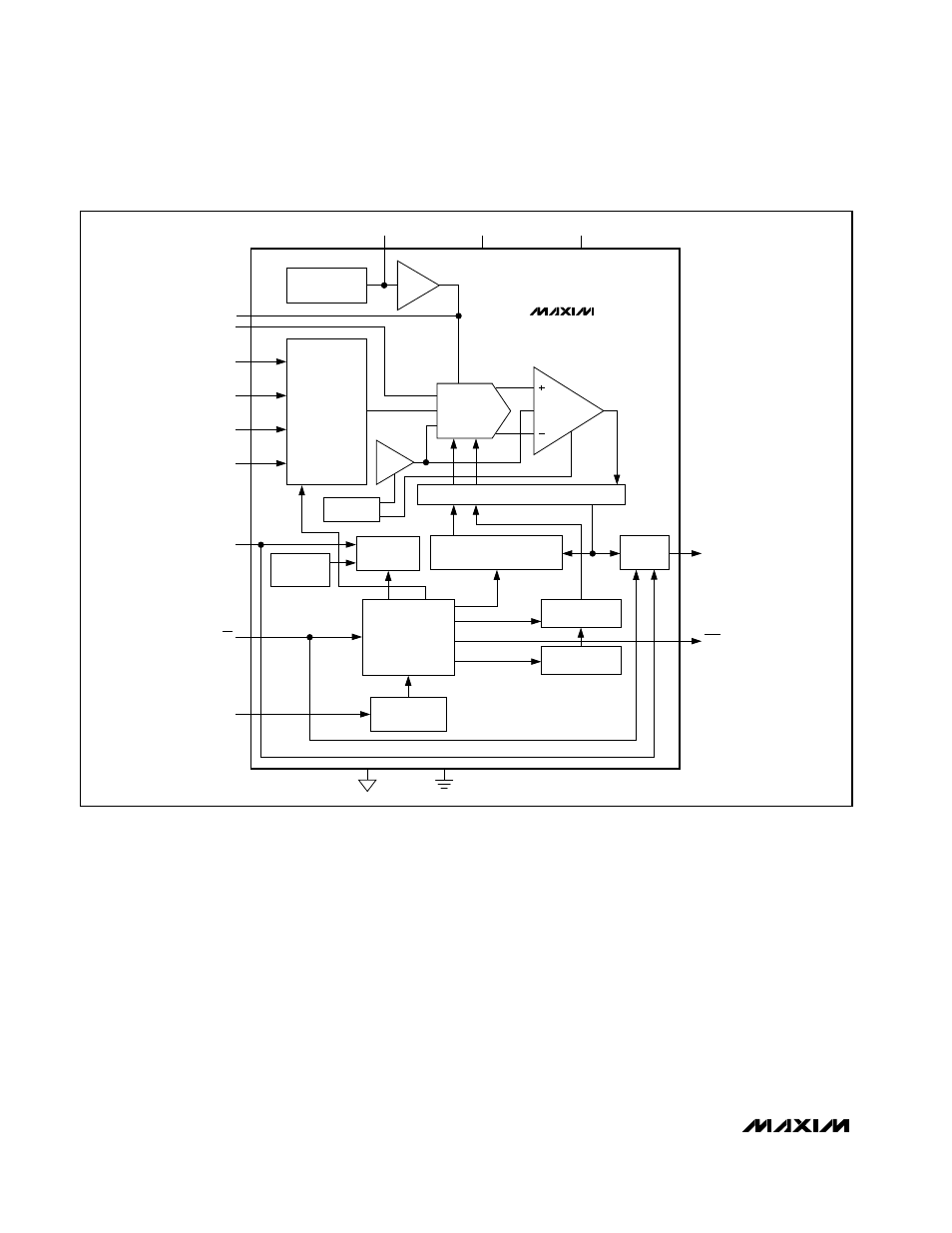
REFERENCE
REF
REFCAP
AV
DD
DV
DD
AGND
AGND
DGND
AIN0
AIN1
AIN2
AIN3
SCLK
CS
DIN
ANALOG-INPUT
MULTIPLEXER
MULTIPLEXER
CONTROL
ACCUMULATOR
MEMORY
INPUT REGISTER
BIAS
OSCILLATOR
OUTPUT
DOUT
EOC
ANALOG-SWITCH FINE TIMING
SUCCESSIVE-APPROXIMATION
REGISTER
MAX1167
DAC
BUFFER
AZ
RAIL
COMPARATOR
Figure 3. MAX1167 Functional Diagram