Pin description, Functional diagram, Typical operating characteristics (continued) – Rainbow Electronics MAX1364 User Manual
Page 8
MAX1363/MAX1364
4-Channel, 12-Bit System Monitors with Programmable
Trip Window and SMBus Alert Response
8
_______________________________________________________________________________________
PIN
NAME
FUNCTION
1
AIN0
Analog Input
2
AIN1
Analog Input
3
AIN2
Analog Input
4
AIN3/V
REF
Analog Input or Reference Input or Output. See Table 3.
5
A0
I
2
C Address Select Input. Connect to V
DD
or GND. See Table 1.
6
INT
Active-Low, Open-Drain Interrupt Output
7
SCL
I
2
C Clock Input
8
SDA
I
2
C Data Input/Output
9
GND
Ground
10
V
DD
Positive Supply Voltage. Bypass V
DD
to GND with a 0.1µF capacitor.
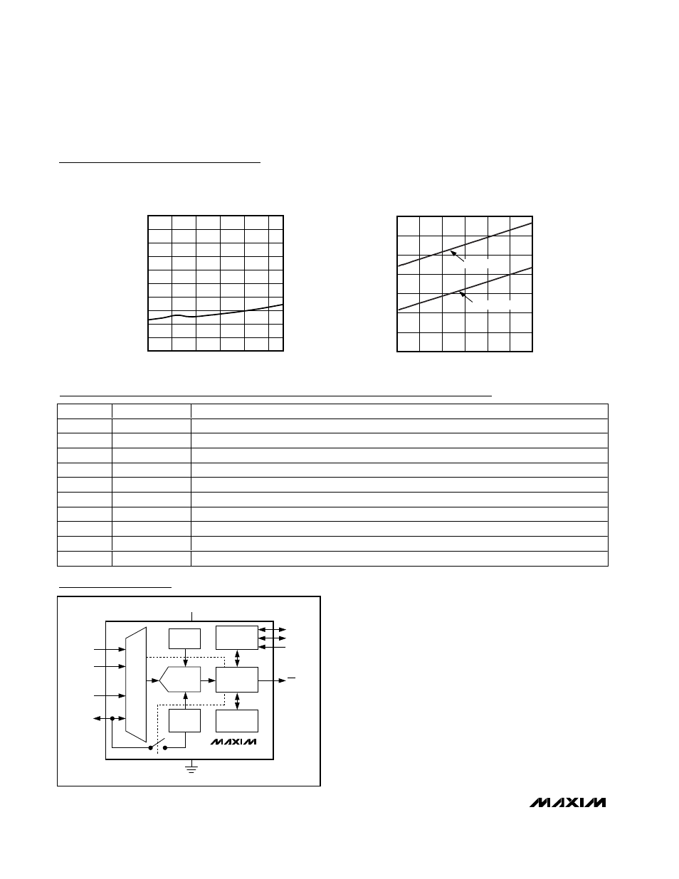
Pin Description
MAX1363/MAX1364
12-BIT
ADC
4:1
MUX
CONTROL
TRIP
THRESHOLDS
I
2
C
INTERFACE
SDA
SCL
A0
INT
CLK
INT
REF
GND
V
DD
AIN0
AIN1
AIN2
AIN3/
REF
Functional Diagram
0
0.3
0.2
0.1
0.4
0.5
0.6
0.7
0.8
0.9
1.0
2.7
3.7
3.2
4.2
4.7
5.2
GAIN ERROR vs. SUPPLY VOLTAGE
MAX1363/64 toc13
V
DD
(V)
GAIN ERROR (LSB)
MONITOR-MODE SUPPLY CURRENT
vs. SPEED
MAX1363/64 toc14
SPEED (ksps)
SUPPLY CURRENT (
µ
A)
125
100
75
50
25
100
200
300
400
500
600
700
0
0
150
INTERNAL REF
EXTERNAL REF
Typical Operating Characteristics (continued)
(V
DD
= 3.3V (MAX1363), V
DD
= 5V (MAX1364), f
SCL
= 1.7MHz, external clock, f
SAMPLE
= 94.4ksps, single-ended, unipolar,
T
A
= +25°C, unless otherwise noted.)