Typical operating characteristics, Electrical characteristics (continued) – Rainbow Electronics MAX1364 User Manual
Page 6
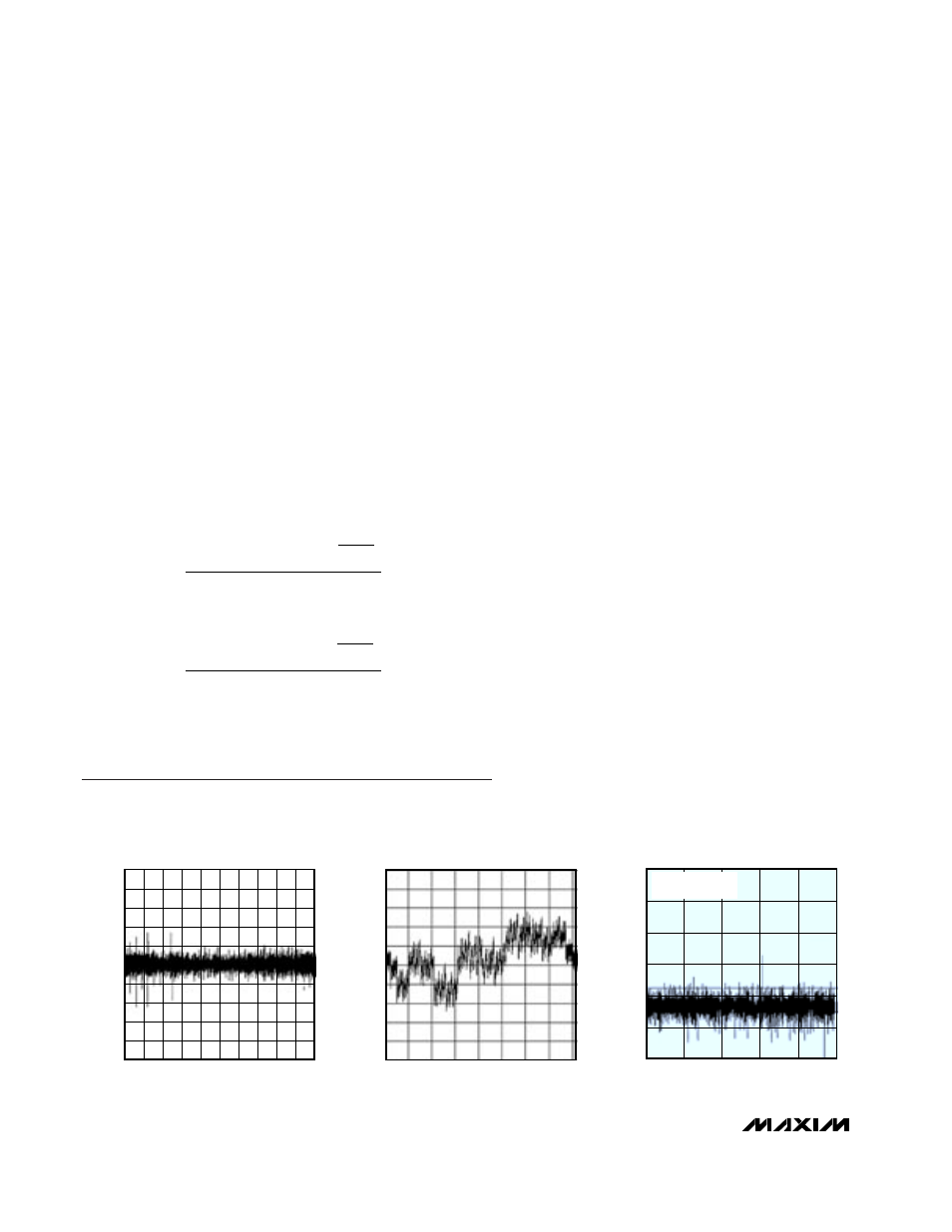
Typical Operating Characteristics
(V
DD
= 3.3V (MAX1363), V
DD
= 5V (MAX1364), f
SCL
= 1.7MHz, external clock, f
SAMPLE
= 94.4ksps, single-ended, unipolar,
T
A
= +25°C, unless otherwise noted.)
MAX1363/MAX1364
4-Channel, 12-Bit System Monitors with Programmable
Trip Window and SMBus Alert Response
6
_______________________________________________________________________________________
ELECTRICAL CHARACTERISTICS (continued)
(V
DD
= 2.7V to 3.6V (MAX1363), V
DD
= 4.5V to 5.5V (MAX1364), V
REF
= 2.048V (MAX1363), V
REF
= 4.096V (MAX1364), C
REF
=
0.1µF, f
SCL
= 1.7MHz, T
A
= T
MIN
to T
MAX
, unless otherwise noted. Typical values are at T
A
= +25°C.)
Note 1:
Devices configured for unipolar single-ended inputs.
Note 2:
Relative accuracy is the deviation of the analog value at any code from its theoretical value after the gain and offset have
been calibrated.
Note 3:
Offset nulled.
Note 4:
Conversion time is defined as the number of clock cycles needed for conversion multiplied by the clock period.
Conversion time does not include acquisition time. SCL is the conversion clock in the external clock mode.
Note 5:
The throughput rate of the I
2
C bus is limited to 94.4ksps. The MAX1363/MAX1364 can perform conversions up to 133ksps
in monitor mode when not reading back results on the I
2
C bus.
Note 6:
A filter on the SDA and SCL inputs suppresses noise spikes and delays the sampling instant.
Note 7:
The absolute input-voltage range for the analog inputs (AIN0–AIN3) is from GND to V
DD
.
Note 8:
When the internal reference is configured to be available at AIN3/REF (SEL[2:1] = 11), decouple AIN3/REF to GND with a
0.01µF capacitor.
Note 9:
ADC performance is limited by the converter’s noise floor, typically 300µV
P-P
.
Note 10:
Maximum conversion throughput in internal clock mode when the data is not clocked out.
Note 11:
For the MAX1363, PSRR is measured as
and for the MAX1364, PSRR is measured as
Note 12:
C
B
= total capacitance of one bus line in pF.
Note 13:
f
SCLH
must meet the minimum clock low time plus the rise/fall times.
Note 14:
A master device must provide a data hold time for SDA (referred to V
IL
of SCL) to bridge the undefined region of SCL’s
falling edge.
V
V
V
V
V
V
V
FS
FS
N
REF
( .
)
( .
)
( .
.
)
5 5
4 5
2
1
5 5
4 5
−
[
]
×
−
−
V
V
V
V
V
V
V
FS
FS
N
REF
( .
)
( .
)
( .
.
)
3 6
2 7
2
1
3 6
2 7
−
[
]
×
−
−
-180
-160
-140
-120
-100
-80
-60
0
10
20
30
40
50
FFT PLOT
MAX1363/64 toc03
FREQUENCY (kHz)
AMPLITUDE (dBc)
f
SAMPLE
= 94.4ksps
f
IN
= 10kHz
-0.5
-0.2
-0.4
-0.3
0.2
0.1
-0.1
0
0.3
0.5
0
4000
DIFFERENTIAL NONLINEARITY
vs. DIGITAL CODE
MAX1363/64 toc01
DIGITAL OUTPUT CODE
DNL (LSB)
1000 1500
500
2000 2500 3000 3500
0.4
-1.0
-0.4
-0.6
-0.8
-0.2
0
0.2
0.4
0.6
0.8
1.0
INTEGRAL NONLINEARITY
vs. DIGITAL CODE
MAX1363/64 toc02
DIGITAL OUTPUT CODE
INL (LSB)
0
4000
1000 1500
500
2000 2500 3000 3500