Rainbow Electronics MAX1364 User Manual
Page 21
Resetting Alarm
Reset alarms by writing to monitor-setup data. See the
Configuring Monitor Mode section and Table 10.
SMBus Alert
The SMBus-alert feature provides a quick method to
identify alarming devices on a shared interrupt. Upon
receiving an interrupt signal, the host µC can broadcast
a receive byte request to the alert-response slave
address (0001100). Any slave device that generated an
interrupt attempts to identify itself by putting its own
address on the bus. The alert response can activate
several different slave devices simultaneously. If more
than one slave attempts to respond, bus arbitration
rules apply, and the device with the lower address wins
as a consequence of the open-collector bus. The losing
device does not generate an acknowledgement and
continues to hold the alert line low until serviced.
Successful reading of the alert response address de-
asserts INT.
When the MAX1363/MAX1364 successfully send the
I
2
C address, it can resume and reassert INT right away
(if the fault is still present). To prevent this from happen-
ing, monitor mode does not resume until after the host
controller resets the alarm in the alarm status register.
Any alarms not cleared when the device resumes moni-
tor mode reassert INT.
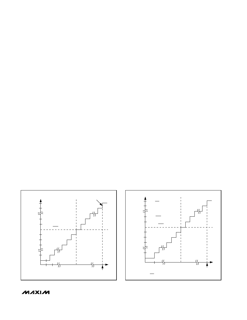
Transfer Functions
Output data coding for the MAX1363/MAX1364 is bina-
ry in unipolar mode and two’s complement in bipolar
mode with 1 LSB = V
REF
/ 2
N
, where N is the number of
bits. Code transitions occur halfway between succes-
sive-integer LSB values. Figures 14 and 15 show the
transfer functions for unipolar and bipolar operations,
respectively.
Layout, Grounding, and Bypassing
Only use PC boards. Wire-wrap configurations are not
recommended since the layout should ensure proper
separation of analog and digital traces. Do not run ana-
log and digital lines parallel to each other, and do not
layout digital signal paths underneath the ADC pack-
age. Use separate analog and digital PC board ground
sections with only one star point (Figure 16).
High-frequency noise in the power supply (V
DD
) could
influence the proper operation of the ADC’s fast com-
parator. Bypass V
DD
to the star ground with a network
of two parallel capacitors, 0.1µF and 4.7µF, located as
close as possible to the MAX1363/MAX1364 power sup-
ply. Minimize capacitor lead length for best supply noise
rejection. For extremely noisy supplies, add an attenua-
tion resistor (5Ω) in series with the power supply.
MAX1363/MAX1364
4-Channel, 12-Bit System Monitors with Programmable
Trip Window and SMBus Alert Response
______________________________________________________________________________________
21
111...111
OUTPUT CODE
FS = REF + GND
ZS = GND
FULL-SCALE
TRANSITION
111...110
100...010
100...001
100...000
011...111
011...110
011...101
000...001
000...000
0
1
512
INPUT VOLTAGE (LSB)
(GND)
1 LSB =
V
REF
1024
FS - 0.5 LSB
Figure 14. Unipolar Transfer Function
011...111
OUTPUT CODE
ZS = AIN-
011...110
000...010
000...001
000...000
111...111
111...110
111...101
100...001
100...000
AIN-
INPUT VOLTAGE (LSB)
+FS - 1 LSB
1 LSB =
V
REF
1024
AIN- ≥
V
REF
2
FS =
V
REF
+ AIN-
2
-FS =
-V
REF
+ AIN-
2
-FS + 0.5 LSB
Figure 15. Bipolar Transfer Function