Electrical characteristics (continued) – Rainbow Electronics MAX1364 User Manual
Page 5
MAX1363/MAX1364
4-Channel, 12-Bit System Monitors with Programmable
Trip Window and SMBus Alert Response
_______________________________________________________________________________________
5
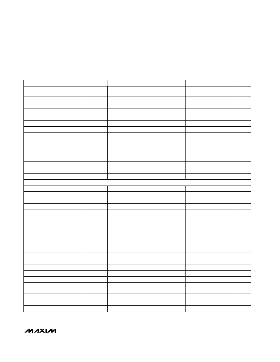
ELECTRICAL CHARACTERISTICS (continued)
(V
DD
= 2.7V to 3.6V (MAX1363), V
DD
= 4.5V to 5.5V (MAX1364), V
REF
= 2.048V (MAX1363), V
REF
= 4.096V (MAX1364), C
REF
=
0.1µF, f
SCL
= 1.7MHz, T
A
= T
MIN
to T
MAX
, unless otherwise noted. Typical values are at T
A
= +25°C.)
PARAMETER
SYMBOL
CONDITIONS
MIN
TYP
MAX
UNITS
Hold Time for START (S)
Condition
t
HD, STA
0.6
µs
Low Period of the SCL Clock
t
LOW
1.3
µs
High Period of the SCL Clock
t
HIGH
0.6
µs
Setup Time for a Repeated
START Condition (Sr)
t
SU, STA
0.6
µs
Data Hold Time
t
HD, DAT
0
900
ns
Data Setup Time
t
SU, DAT
100
ns
Rise Time of Both SDA and SCL
Signals, Receiving
t
R
Measured from 0.3V
DD
to 0.7V
DD
0
300
ns
Fall Time of SDA Transmitting
t
F
Measured from 0.3V
DD
to 0.7V
DD
0
300
ns
Setup Time for STOP (P)
Condition
t
SU, STO
0.6
µs
Capacitive Load for Each Bus
Line
C
B
400
pF
Pulse Width of Spike Suppressed
50
ns
TIMING CHARACTERISTICS FOR HIGH-SPEED MODE (C
B
= 400pF, Figures 1a, 2) (Note 12)
Serial Clock Frequency
f
SCLH
(Note 13)
1.7
MHz
Hold Time, Repeated START
Condition (Sr)
t
HD, STA
160
ns
Low Period of the SCL Clock
t
LOW
(Note 13)
320
ns
High Period of the SCL Clock
t
HIGH
120
ns
Setup Time for a Repeated
START Condition (Sr)
t
SU, STA
160
ns
Data Hold Time
t
HD, DAT
(Note 14)
0
150
ns
Data Setup Time
t
SU, DAT
10
ns
Rise Time of SCL Signal, Current
Source Enabled
t
RCL
Measured from 0.3V
DD
to 0.7V
DD
20
80
ns
Rise Time of SCL Signal After
Acknowledge Bit
t
RCL1
Measured from 0.3V
DD
to 0.7V
DD
20
160
ns
Fall Time of SCL Signal
t
FCL
Measured from 0.3V
DD
to 0.7V
DD
20
80
ns
Rise Time of SDA Signal
t
RDA
Measured from 0.3V
DD
to 0.7V
DD
20
160
ns
Fall Time of SDA Signal
t
FDA
Measured from 0.3V
DD
to 0.7V
DD
20
160
ns
Setup Time for STOP (P)
Condition
t
SU, STO
160
ns
Capacitive Load for Each Bus
Line
C
B
(Notes 13, 14)
400
pF
Pulse Width of Spike Suppressed
0
10
ns