Rainbow Electronics MAX1364 User Manual
Page 12
MAX1363/MAX1364
External Clock
See the Configuration/Setup Bytes (Write Cycle) section.
When configured for external clock mode (CLK = 1), the
MAX1363/MAX1364 use SCL as the conversion clock. In
external clock mode, the MAX1363/MAX1364 begin
tracking the analog input on the ninth rising clock edge of
a valid slave address byte. Two SCL clock cycles later,
the analog signal is acquired and the conversion begins.
Unlike internal clock mode, converted data is clocked out
immediately in the format described in the Reading a
Conversion (Read Cycle) section.
The device continuously converts input channels dictat-
ed by the scan mode until given a not acknowledge
(NACK). There is no need to readdress the device with
a read command to obtain new conversion results.
The conversion must complete in 1ms or droop on the
T/H capacitor degrades conversion results. Use inter-
nal clock mode if the SCL clock period exceeds 60µs.
Use external clock mode for conversion rates from
40ksps to 94.4ksps. Use internal clock mode for conver-
sions under 40ksps. Internal clock mode consumes less
power. Monitor mode always uses internal clock mode.
Applications Section
Power-On Reset
The configuration and setup registers default to a sin-
gle-ended, unipolar, single-channel conversion on
AIN0 using the internal clock with V
DD
as the reference
and AIN3/REF configured as an analog input. The
memory contents are unknown at power-up (see the
Software Description section).
I
2
C-Compatible 2-Wire Serial Interface
The MAX1363/MAX1364 use an I
2
C-compatible 2-wire
interface consisting of a serial data line (SDA) and serial
clock line (SCL). SDA and SCL facilitate bidirectional
communication between the MAX1363/MAX1364 and
the master at rates up to 1.7MHz. The master (typically
a µC) initiates data transfer on the bus and generates
the SCL signal to permit data transfer. The MAX1363/
MAX1364 behave as I
2
C slave devices that transfer and
receive data.
SDA and SCL must be pulled high for proper I
2
C oper-
ation. This is typically done with pullup resistors (750Ω
or greater). Series resistors (R
S
) are optional (see the
Typical Operating Circuit section). The resistors protect
the input architecture of the MAX1363/MAX1364 from
high voltage spikes on the bus lines and minimize
crosstalk and undershoot of the bus signals.
One bit transfers during each SCL clock cycle. A mini-
mum of nine clock cycles is required to transfer a byte
in or out of the MAX1363/MAX1364 (8 bits and an
ACK/NACK). The data on SDA must remain stable dur-
ing the high period of the SCL clock pulse. Changes in
SDA while SCL is stable and high are considered con-
trol signals (see the START and STOP Conditions sec-
tion). Both SDA and SCL remain high when the bus is
not busy.
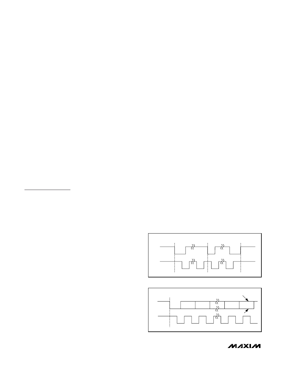
START and STOP Conditions
The master initiates a transmission with a START condi-
tion (S), which is a high-to-low transition on SDA while
SCL is high. The master terminates a transmission with
a STOP condition (P), which is a low-to-high transition
on SDA while SCL is high (Figure 4). A repeated START
condition (Sr) can be used in place of a STOP condition
to leave the bus active and the mode unchanged (see
the HS I
2
C Mode section).
Acknowledge and Not-Acknowledge Conditions
Data transfers are framed with an acknowledge bit
(ACK) or a not-acknowledge bit (NACK). Both the mas-
ter and the MAX1363/MAX1364 (slave) generate
acknowledge bits. To generate an acknowledge, the
receiving device must pull SDA low before the rising
edge of the acknowledge-related clock pulse (ninth
pulse) and keep it low during the high period of the
clock pulse (Figure 5).
To generate a not-acknowledge condition, the receiver
allows SDA to be pulled high before the rising edge of
the acknowledge-related clock pulse, and leaves SDA
high during the high period of the clock pulse.
Monitoring the acknowledge bits allows for detection of
4-Channel, 12-Bit System Monitors with Programmable
Trip Window and SMBus Alert Response
12
______________________________________________________________________________________
SCL
SDA
S
P
Sr
Figure 4. START and STOP Conditions
SCL
SDA
S
NOT ACKNOWLEDGE
ACKNOWLEDGE
1
2
8
9
Figure 5. Acknowledge Bits