Input bandwidth, Analog input protection, Quick look – Rainbow Electronics MAX149 User Manual
Page 9
MAX148/MAX149
+2.7V to +5.25V, Low-Power, 8-Channel,
Serial 10-Bit ADCs
_______________________________________________________________________________________
9
allowed between conversions. The acquisition time,
t
ACQ
, is the maximum time the device takes to acquire
the signal, and is also the minimum time needed for the
signal to be acquired. It is calculated by the following
equation:
t
ACQ
= 7 x (R
S
+ R
IN
) x 16pF
where R
IN
= 9k
Ω
, R
S
= the source impedance of the
input signal, and t
ACQ
is never less than 1.5µs. Note
that source impedances below 4k
Ω
do not significantly
affect the ADC’s AC performance.
Higher source impedances can be used if a 0.01µF
capacitor is connected to the individual analog inputs.
Note that the input capacitor forms an RC filter with the
input source impedance, limiting the ADC’s signal
bandwidth.
Input Bandwidth
The ADC’s input tracking circuitry has a 2.25MHz
small-signal bandwidth, so it is possible to digitize
high-speed transient events and measure periodic sig-
nals with bandwidths exceeding the ADC’s sampling
rate by using undersampling techniques. To avoid
high-frequency signals being aliased into the frequency
band of interest, anti-alias filtering is recommended.
Analog Input Protection
Internal protection diodes, which clamp the analog input
to V
DD
and AGND, allow the channel input pins to swing
from AGND - 0.3V to V
DD
+ 0.3V without damage.
However, for accurate conversions near full scale, the
inputs must not exceed V
DD
by more than 50mV or be
lower than AGND by 50mV.
If the analog input exceeds 50mV beyond the sup-
plies, do not forward bias the protection diodes of
off channels over 2mA.
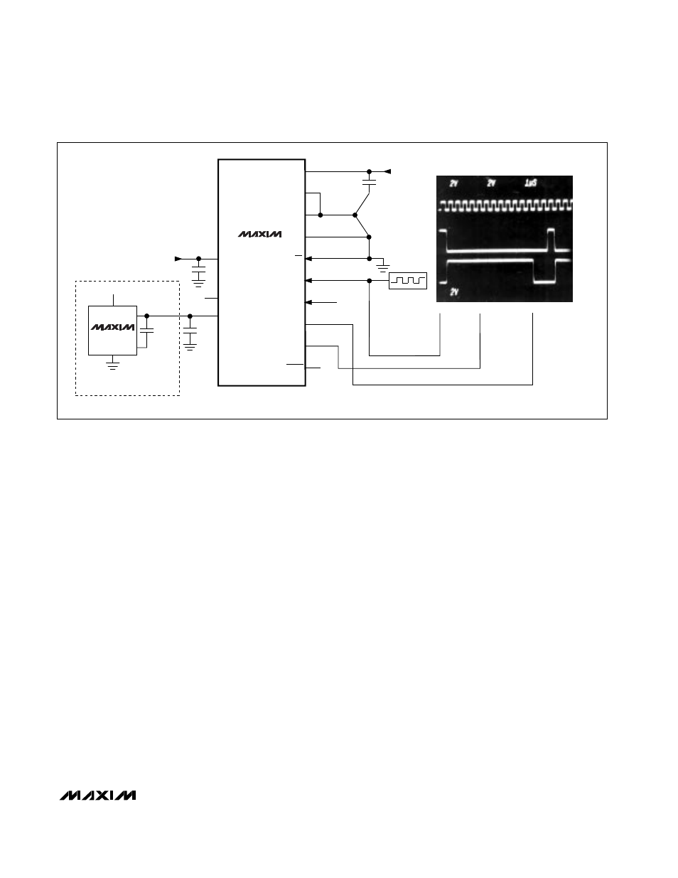
Quick Look
To quickly evaluate the MAX148/MAX149’s analog perfor-
mance, use the circuit of Figure 5. The MAX148/MAX149
require a control byte to be written to DIN before each
conversion. Tying DIN to +3V feeds in control bytes of
$FF (HEX), which trigger single-ended unipolar conver-
sions on CH7 in external clock mode without powering
down between conversions. In external clock mode, the
SSTRB output pulses high for one clock period before
the most significant bit of the conversion result is shift-
ed out of DOUT. Varying the analog input to CH7 will
alter the sequence of bits from DOUT. A total of 15
clock cycles is required per conversion. All transitions
of the SSTRB and DOUT outputs occur on the falling
edge of SCLK.
0.1µF
V
DD
DGND
AGND
COM
CS
SCLK
DIN
DOUT
SSTRB
SHDN
+3V
N.C.
0.01µF
CH7
+3V
REFADJ
VREF
C1
0.1µF
0V TO
+2.500V
ANALOG
INPUT
OSCILLOSCOPE
CH1
CH2
CH3
CH4
* FULL-SCALE ANALOG INPUT, CONVERSION RESULT = $FFF (HEX)
OPTIONAL FOR MAX149,
REQUIRED FOR MAX148
MAX148
MAX149
+3V
2MHz
OSCILLATOR
SCLK
SSTRB
DOUT*
2.5V
1000pF
COMP
V
OUT
+3V
MAX872
Figure 5. Quick-Look Circuit