Rainbow Electronics MAX149 User Manual
Page 10
MAX148/MAX149
+2.7V to +5.25V, Low-Power, 8-Channel,
Serial 10-Bit ADCs
10
______________________________________________________________________________________
How to Start a Conversion
Start a conversion by clocking a control byte into DIN.
With CS low, each rising edge on SCLK clocks a bit from
DIN into the MAX148/MAX149’s internal shift register.
After CS falls, the first arriving logic “1” bit defines the
control byte’s MSB. Until this first “start” bit arrives, any
number of logic “0” bits can be clocked into DIN with no
effect. Table 1 shows the control-byte format.
The MAX148/MAX149 are compatible with SPI/
QSPI and MICROWIRE devices. For SPI, select the cor-
rect clock polarity and sampling edge in the SPI control
registers: set CPOL = 0 and CPHA = 0. MICROWIRE,
SPI, and QSPI all transmit a byte and receive a byte at
the same time. Using the
Typical Operating Circuit,
the
simplest software interface requires only three 8-bit
transfers to perform a conversion (one 8-bit transfer to
configure the ADC, and two more 8-bit transfers to clock
out the conversion result). See Figure 20 for MAX148/
MAX149 QSPI connections.
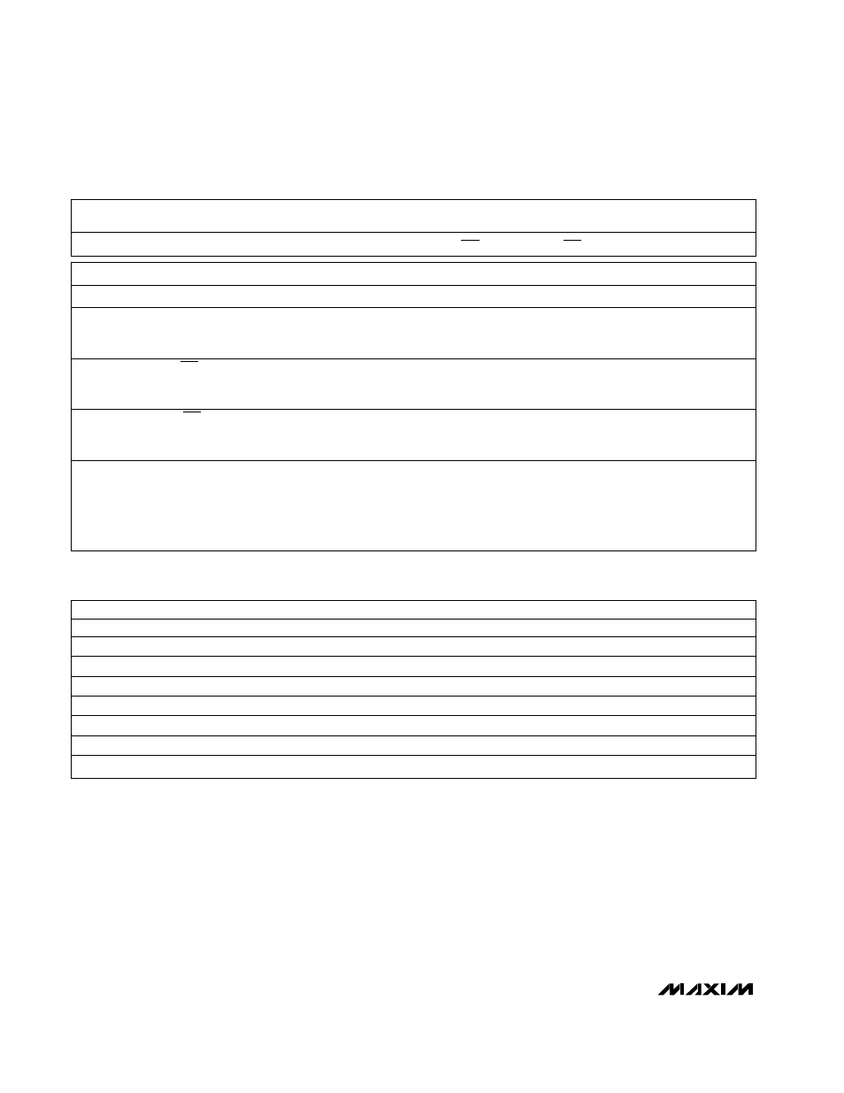
BIT
NAME
DESCRIPTION
7(MSB)
START
The first logic “1” bit after CS goes low defines the beginning of the control byte.
6
SEL2
These three bits select which of the eight channels are used for the conversion (Tables 2 and 3).
5
SEL1
4
SEL0
3
UNI/BIP
1 = unipolar, 0 = bipolar. Selects unipolar or bipolar conversion mode. In unipolar mode, an
analog input signal from 0V to VREF can be converted; in bipolar mode, the signal can range
from -VREF/2 to +VREF/2.
2
SGL/DIF
1 = single ended, 0 = differential. Selects single-ended or differential conversions. In single-
ended mode, input signal voltages are referred to COM. In differential mode, the voltage
difference between two channels is measured (Tables 2 and 3).
1
PD1
Selects clock and power-down modes.
0(LSB)
PD0
PD1
PD0
Mode
0
0
Full power-down
0
1
Fast power-down (MAX149 only)
1
0
Internal clock mode
1
1
External clock mode
Table 1. Control-Byte Format
BIT 7
BIT 6
BIT 5
BIT 4
BIT 3
BIT 2
BIT 1
BIT 0
(MSB)
(LSB)
START
SEL2
SEL1
SEL0
UNI/BIP
SGL/DIF
PD1
PD0
SEL2
SEL1
SEL0
CH0
CH1
CH2
CH3
CH4
CH5
CH6
CH7
COM
0
0
0
+
–
1
0
0
+
–
0
0
1
+
–
1
0
1
+
–
0
1
0
+
–
1
1
0
+
–
0
1
1
+
–
1
1
1
+
–
Table 2. Channel Selection in Single-Ended Mode (SGL/
D
DIIF
F
= 1)