External clock, Internal clock – Rainbow Electronics MAX149 User Manual
Page 12
MAX148/MAX149
+2.7V to +5.25V, Low-Power, 8-Channel,
Serial 10-Bit ADCs
12
______________________________________________________________________________________
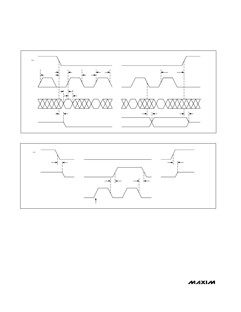
MAX148/MAX149. The T/H acquires the input signal as
the last three bits of the control byte are clocked into
DIN. Bits PD1 and PD0 of the control byte program the
clock mode. Figures 7–10 show the timing characteris-
tics common to both modes.
External Clock
In external clock mode, the external clock not only shifts
data in and out, but it also drives the analog-to-digital
conversion steps. SSTRB pulses high for one clock
period after the last bit of the control byte. Succes-
sive-approximation bit decisions are made and appear
at DOUT on each of the next 12 SCLK falling edges
(Figure 6). SSTRB and DOUT go into a high-impedance
state when CS goes high; after the next CS falling edge,
SSTRB outputs a logic low. Figure 8 shows the SSTRB
timing in external clock mode.
The conversion must complete in some minimum time,
or droop on the sample-and-hold capacitors may
degrade conversion results. Use internal clock mode if
the serial-clock frequency is less than 100kHz, or if
serial-clock interruptions could cause the conversion
interval to exceed 120µs.
Internal Clock
In internal clock mode, the MAX148/MAX149 generate
their own conversion clocks internally. This frees the µP
• • •
• • •
• • •
• • •
t
SDV
t
SSTRB
PD0 CLOCKED IN
t
STR
SSTRB
SCLK
CS
t
SSTRB
• • •
• • • •
•
Figure 8. External Clock Mode SSTRB Detailed Timing
• • •
• • •
• • •
• • •
CS
SCLK
DIN
DOUT
t
CSH
t
CSS
t
CL
t
DS
t
DH
t
DV
t
CH
t
DO
t
TR
t
CSH
Figure 7. Detailed Serial-Interface Timing