Internal and external references, Lowest power at higher throughputs, Internal reference (max149) – Rainbow Electronics MAX149 User Manual
Page 18: External reference
MAX148/MAX149
+2.7V to +5.25V, Low-Power, 8-Channel,
Serial 10-Bit ADCs
18
______________________________________________________________________________________
Lowest Power at Higher Throughputs
Figure 14b shows the power consumption with
external-reference compensation in fast power-down,
with one and eight channels converted. The external
4.7µF compensation requires a 75µs wait after
power-up with one dummy conversion. This graph
shows fast multi-channel conversion with the lowest
power consumption possible. Full power-down mode
may provide increased power savings in applications
where the MAX148/MAX149 are inactive for long peri-
ods of time, but where intermittent bursts of high-speed
conversions are required.
Internal and External References
The MAX149 can be used with an internal or external
reference voltage, whereas an external reference is
required for the MAX148. An external reference can be
connected directly at VREF or at the REFADJ pin.
An internal buffer is designed to provide 2.5V at
VREF for both the MAX149 and the MAX148. The
MAX149’s internally trimmed 1.21V reference is buf-
fered with a 2.06 gain. The MAX148’s REFADJ pin is
also buffered with a 2.00 gain to scale an external 1.25V
reference at REFADJ to 2.5V at VREF.
Internal Reference (MAX149)
The MAX149’s full-scale range with the internal refer-
ence is 2.5V with unipolar inputs and ±1.25V with bipo-
lar inputs. The internal reference voltage is adjustable
to ±1.5% with the circuit in Figure 16.
External Reference
With both the MAX149 and MAX148, an external refer-
ence can be placed at either the input (REFADJ) or the
output (VREF) of the internal reference-buffer amplifier.
The REFADJ input impedance is typically 20k
Ω
for the
MAX149, and higher than 100k
Ω
for the MAX148. At
OUTPUT CODE
FULL-SCALE
TRANSITION
11 . . . 111
11 . . . 110
11 . . . 101
00 . . . 011
00 . . . 010
00 . . . 001
00 . . . 000
1
2
3
0
(COM)
FS
FS - 3/2LSB
FS = VREF + COM
ZS = COM
INPUT VOLTAGE (LSB)
1LSB =
VREF
1024
Figure 17. Unipolar Transfer Function, Full Scale (FS) = VREF
+ COM, Zero Scale (ZS) = COM
+3.3V
510k
24k
100k
0.01µF
12
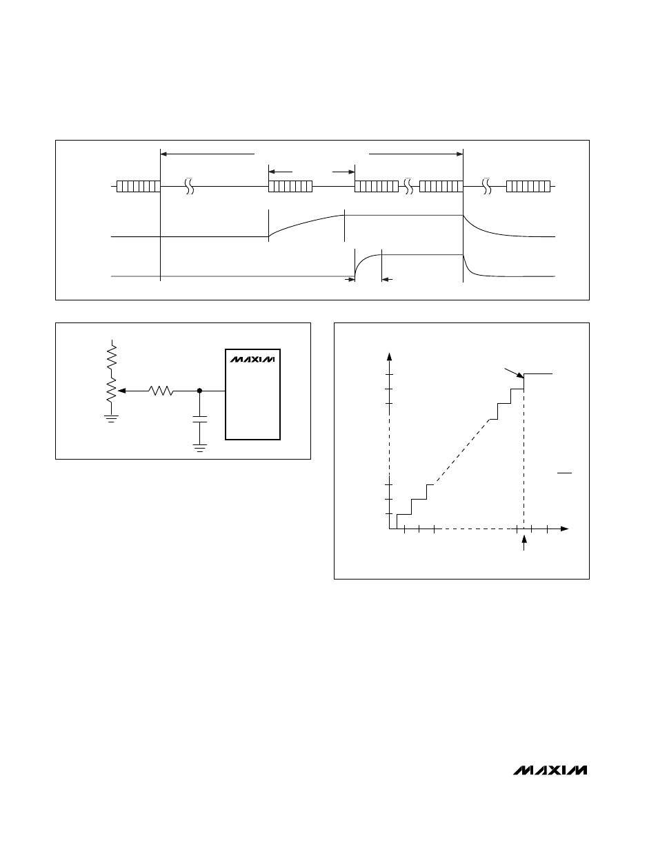
REFADJ
MAX149
Figure 16. MAX149 Reference-Adjust Circuit
1
0 0
DIN
REFADJ
VREF
1.21V
0V
2.50V
0V
1
0 1
1
1
1
1
0 0
1
0 1
FULLPD
FASTPD
NOPD
FULLPD
FASTPD
1.6ms WAIT
COMPLETE CONVERSION SEQUENCE
t
BUFFEN
≈
75
µ
s
τ
= RC = 20k
Ω
x C
REFADJ
(ZEROS)
CH1
CH7
(ZEROS)
Figure 15. MAX149 FULLPD/FASTPD Power-Up Sequence