Layout, grounding, and bypassing – Rainbow Electronics MAX149 User Manual
Page 20
MAX148/MAX149
+2.7V to +5.25V, Low-Power, 8-Channel,
Serial 10-Bit ADCs
20
______________________________________________________________________________________
Layout, Grounding, and Bypassing
For best performance, use printed circuit boards.
Wire-wrap boards are not recommended. Board layout
should ensure that digital and analog signal lines are
separated from each other. Do not run analog and digi-
tal (especially clock) lines parallel to one another, or
digital lines underneath the ADC package.
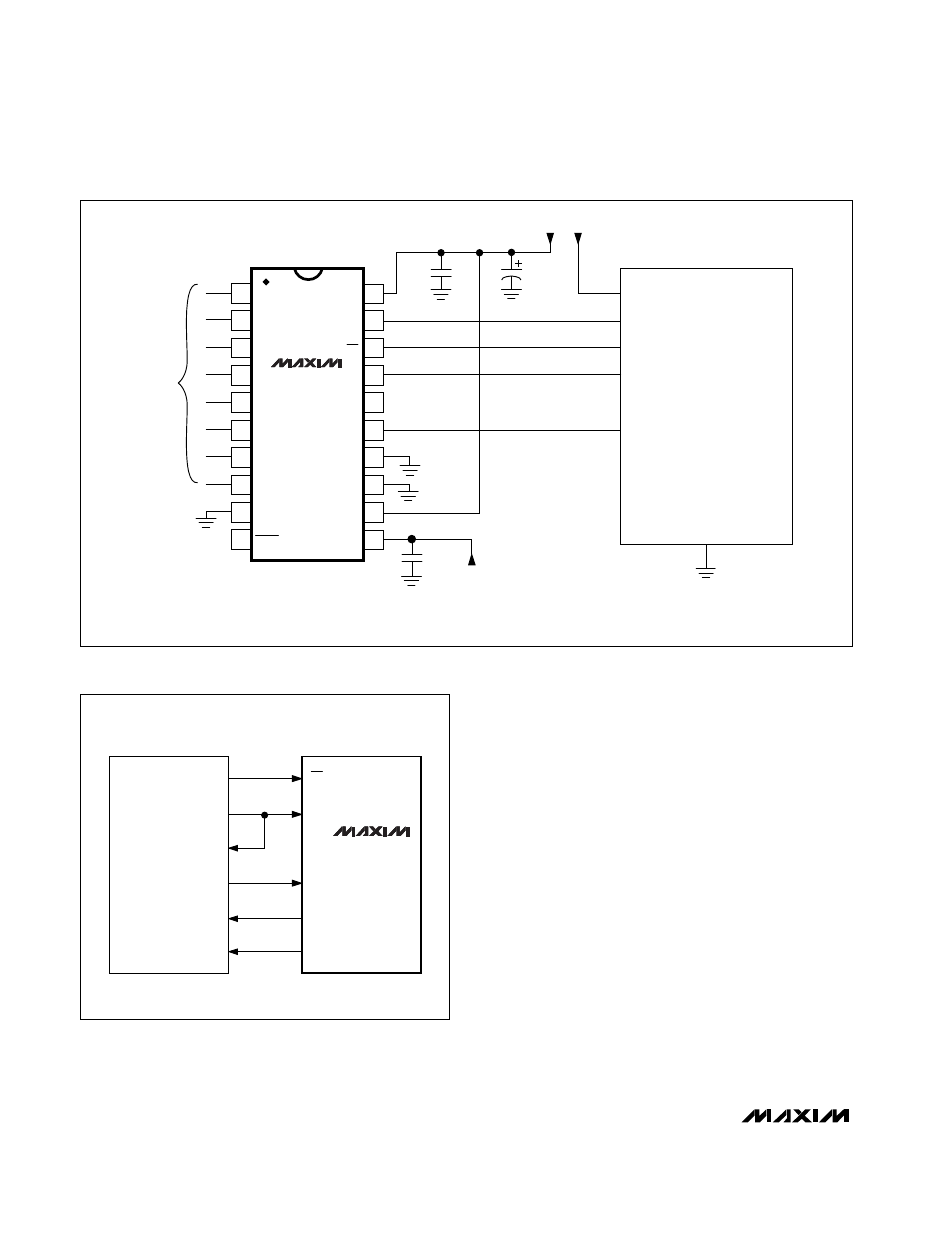
Figure 19 shows the recommended system ground
connections. Establish a single-point analog ground
(star ground point) at AGND, separate from the logic
ground. Connect all other analog grounds and DGND
to the star ground. No other digital system ground
should be connected to this ground. For lowest-noise
operation, the ground return to the star ground’s power
supply should be low impedance and as short as
possible.
High-frequency noise in the V
DD
power supply may
affect the high-speed comparator in the ADC. Bypass
the supply to the star ground with 0.1µF and 1µF
capacitors close to pin 20 of the MAX148/MAX149.
Minimize capacitor lead lengths for best supply-noise
rejection. If the power supply is very noisy, a 10
Ω
resis-
tor can be connected as a lowpass filter (Figure 19).
20
19
18
17
16
15
14
13
12
11
1
2
3
4
5
6
7
8
9
10
MAX148
MAX149
MC683XX
CH0
CH1
CH2
CH3
CH4
CH5
CH6
CH7
COM
SHDN
V
DD
SCLK
CS
DIN
SSTRB
DOUT
DGND
AGND
REFADJ
VREF
(POWER SUPPLIES)
SCK
PCS0
MOSI
MISO
0.1
µ
F
1
µ
F
(GND)
0.1
µ
F
ANALOG
INPUTS
+3V
+3V
+2.5V
Figure 20. MAX148/MAX149 QSPI Connections, External Reference
XF
CLKX
CLKR
DX
DR
FSR
CS
SCLK
DIN
DOUT
SSTRB
TMS320LC3x
MAX148
MAX149
Figure 21. MAX148/MAX149-to-TMS320 Serial Interface