Transfer function, Table 7. full scale and zero scale – Rainbow Electronics MAX149 User Manual
Page 19
MAX148/MAX149
+2.7V to +5.25V, Low-Power, 8-Channel,
Serial 10-Bit ADCs
______________________________________________________________________________________
19
VREF, the DC input resistance is a minimum of 18k
Ω
.
During conversion, an external reference at VREF must
deliver up to 350µA DC load current and have 10
Ω
or
less output impedance. If the reference has a higher
output impedance or is noisy, bypass it close to the
VREF pin with a 4.7µF capacitor.
Using the REFADJ input makes buffering the external
reference unnecessary. To use the direct VREF input,
disable the internal buffer by tying REFADJ to V
DD
. In
power-down, the input bias current to REFADJ is typi-
cally 25µA (MAX149) with REFADJ tied to V
DD
. Pull
REFADJ to AGND to minimize the input bias current in
power-down.
Transfer Function
Table 7 shows the full-scale voltage ranges for unipolar
and bipolar modes.
The external reference must have a temperature coeffi-
cient of 20ppm/°C or less to achieve accuracy to within
1LSB over the 0°C to +70°C commercial temperature
range.
Figure 17 depicts the nominal, unipolar input/output
(I/O) transfer function, and Figure 18 shows the bipolar
input/output transfer function. Code transitions occur
halfway between successive-integer LSB values.
Output coding is binary, with 1LSB = 2.44mV (2.500V /
1024) for unipolar operation, and 1LSB = 2.44mV
[(2.500V / 2 - -2.500V / 2) / 1024] for bipolar operation.
011 . . . 111
011 . . . 110
000 . . . 010
000 . . . 001
000 . . . 000
111 . . . 111
111 . . . 110
111 . . . 101
100 . . . 001
100 . . . 000
- FS
COM*
INPUT VOLTAGE (LSB)
OUTPUT CODE
ZS = COM
+FS - 1LSB
*COM VREF / 2
+ COM
FS
=
VREF
2
-FS =
+ COM
-VREF
2
1LSB =
VREF
1024
≤
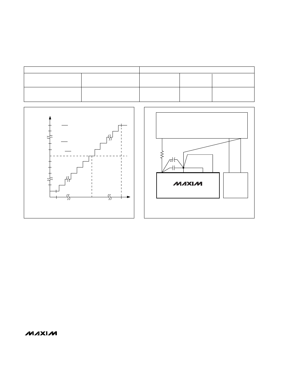
Figure 18. Bipolar Transfer Function, Full Scale (FS) =
VREF / 2 + COM, Zero Scale (ZS) = COM
+3V
+3V
GND
SUPPLIES
DGND
+3V
DGND
COM
AGND
V
DD
DIGITAL
CIRCUITRY
MAX148
MAX149
R* = 10
Ω
*OPTIONAL
Figure 19. Power-Supply Grounding Connection
UNIPOLAR MODE
BIPOLAR MODE
Full Scale
Zero Scale
Positive
Zero
Negative
Full Scale
Scale
Full Scale
VREF + COM
COM
VREF / 2
COM
-VREF / 2
+ COM
+ COM
Table 7. Full Scale and Zero Scale