Rainbow Electronics MAX149 User Manual
Page 17
MAX148/MAX149
+2.7V to +5.25V, Low-Power, 8-Channel,
Serial 10-Bit ADCs
______________________________________________________________________________________
17
Software Power-Down
Software power-down is activated using bits PD1 and PD0
of the control byte. As shown in Table 5, PD1 and PD0
also specify the clock mode. When software shutdown is
asserted, the ADC operates in the last specified clock
mode until the conversion is complete. Then the ADC
powers down into a low quiescent-current state. In internal
clock mode, the interface remains active and conversion
results may be clocked out after the MAX148/MAX149
enter a software power-down.
The first logical 1 on DIN is interpreted as a start bit
and powers up the MAX148/MAX149. Following
the start bit, the data input word or control byte also
determines clock mode and power-down states. For
example, if the DIN word contains PD1 = 1, then the
chip remains powered up. If PD0 = PD1 = 0, a
power-down resumes after one conversion.
Hardware Power-Down
Pulling SHDN low places the converter in hardware
power-down (Table 6). Unlike software power-down
mode, the conversion is not completed; it stops coin-
cidentally with SHDN being brought low. SHDN also
controls the clock frequency in internal clock mode.
Letting SHDN float sets the internal clock frequency to
1.8MHz. When returning to normal operation with SHDN
floating, there is a t
RC
delay of approximately 2M
Ω
x C
L
,
where C
L
is the capacitive loading on the SHDN pin.
Pulling SHDN high sets internal clock frequency to
225kHz. This feature eases the settling-time requirement
for the reference voltage. With an external reference, the
MAX148/MAX149 can be considered fully powered up
within 2µs of actively pulling SHDN high.
Power-Down Sequencing
The MAX148/MAX149 auto power-down modes can
save considerable power when operating at less than
maximum sample rates. Figures 13, 14a, and 14b show
the average supply current as a function of the sam-
pling rate. The following discussion illustrates the vari-
ous power-down sequences.
Lowest Power at up to 500
Conversions/Channel/Second
The following examples show two different power-down
sequences. Other combinations of clock rates, compen-
sation modes, and power-down modes may give lowest
power consumption in other applications.
Figure 14a depicts the MAX149 power consumption for
one or eight channel conversions utilizing full power-
down mode and internal-reference compensation. A
0.01µF bypass capacitor at REFADJ forms an RC filter
with the internal 20k
Ω
reference resistor with a 0.2ms
time constant. To achieve full 10-bit accuracy, 8 time
constants or 1.6ms are required after power-up.
Waiting this 1.6ms in FASTPD mode instead of in full
power-up can reduce power consumption by a factor
of 10 or more. This is achieved by using the sequence
shown in Figure 15.
10,000
1
0.1
1
AVERAGE SUPPLY CURRENT
vs. CONVERSION RATE
(USING FASTPD)
1000
100
10
CONVERSION RATE
(Hz)
AVERAGE SUPPLY CURRENT (
µ
A)
100
1M
10
1k
10k
100k
MAX148/9-F14B
R
LOAD
=
∞
CODE = 1010101000
8 CHANNELS
1 CHANNEL
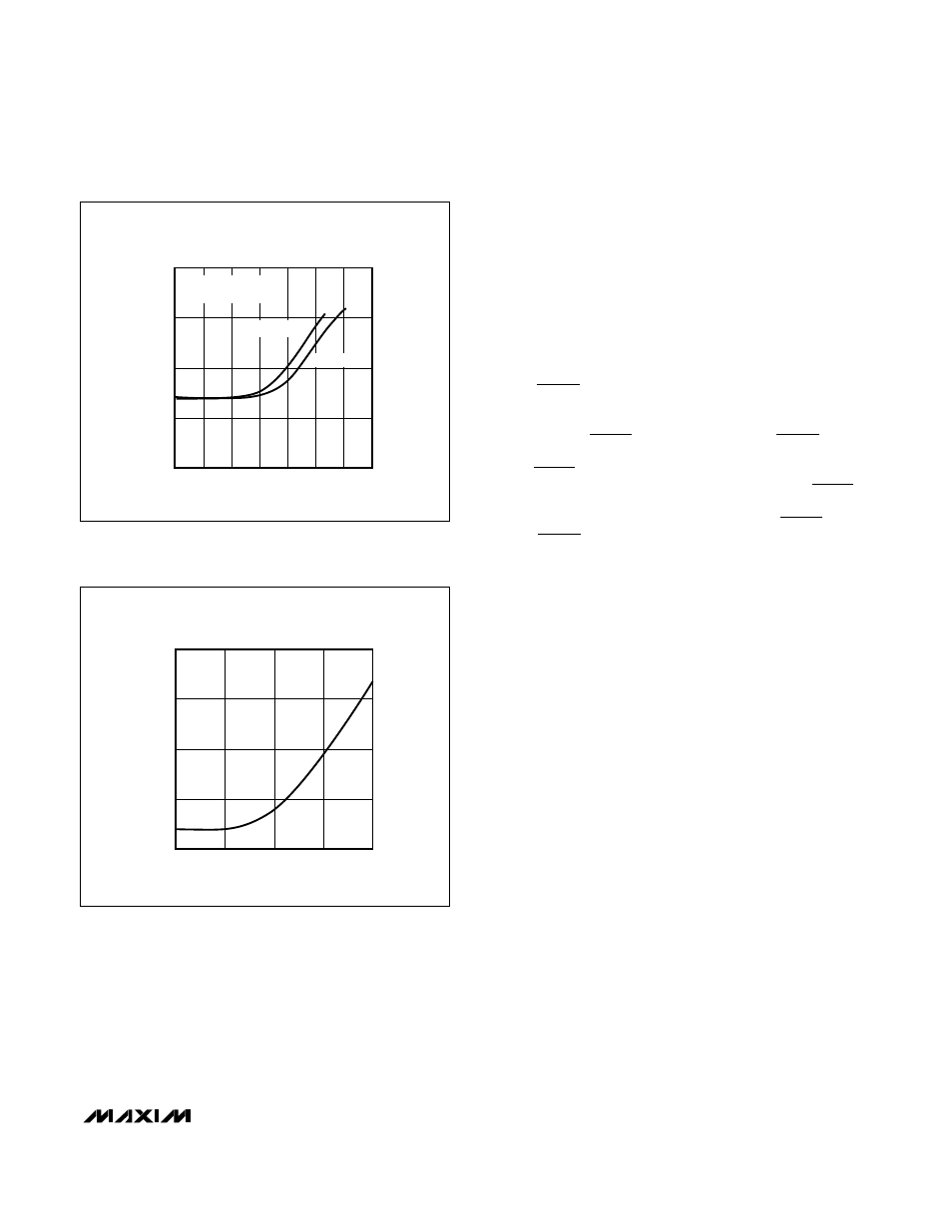
Figure 14c. Typical Reference-Buffer Power-Up Delay vs. Time
in Shutdown
2.0
0
0.001
0.01
0.1
1
10
TYPICAL REFERENCE-BUFFER POWER-UP
DELAY vs. TIME IN SHUTDOWN
1.5
1.0
0.5
TIME IN SHUTDOWN
(sec)
POWER-UP DELAY (ms)
MAX148/9-F14C
Figure 14b. MAX149 Supply Current vs. Conversion Rate,
FASTPD