Applications information – Rainbow Electronics MAX149 User Manual
Page 14
MAX148/MAX149
+2.7V to +5.25V, Low-Power, 8-Channel,
Serial 10-Bit ADCs
14
______________________________________________________________________________________
bit of the control byte (the PD0 bit) is clocked into DIN.
The start bit is defined as follows:
The first high bit clocked into DIN with CS low any
time the converter is idle; e.g., after V
DD
is applied.
OR
The first high bit clocked into DIN after bit 3 of a con-
version in progress is clocked onto the DOUT pin.
If CS is toggled before the current conversion is com-
plete, the next high bit clocked into DIN is recognized as
a start bit; the current conversion is terminated, and a
new one is started.
The fastest the MAX148/MAX149 can run with CS held
low between conversions is 15 clocks per conversion.
Figure 11a shows the serial-interface timing necessary to
perform a conversion every 15 SCLK cycles in external
clock mode. If CS is tied low and SCLK is continuous,
guarantee a start bit by first clocking in 16 zeros.
Most microcontrollers (µCs) require that conversions
occur in multiples of 8 SCLK clocks; 16 clocks per con-
version is typically the fastest that a µC can drive the
MAX148/MAX149. Figure 11b shows the serial-
interface timing necessary to perform a conversion every
16 SCLK cycles in external clock mode.
__________ Applications Information
Power-On Reset
When power is first applied, and if SHDN is not pulled
low, internal power-on reset circuitry activates the
MAX148/MAX149 in internal clock mode, ready to con-
vert with SSTRB = high. After the power supplies stabi-
lize, the internal reset time is 10µs, and no conversions
should be performed during this phase. SSTRB is high
on power-up and, if CS is low, the first logical 1 on DIN
is interpreted as a start bit. Until a conversion takes
place, DOUT shifts out zeros. (Also see Table 4.)
Reference-Buffer Compensation
In addition to its shutdown function, SHDN selects inter-
nal or external compensation. The compensation
affects both power-up time and maximum conversion
speed. The100kHz minimum clock rate is limited by
droop on the sample-and-hold and is independent of
the compensation used.
Float SHDN to select external compensation. The
Typical Operating Circuit
uses a 4.7µF capacitor at
VREF. A 4.7µF value ensures reference-buffer stability
and allows converter operation at the 2MHz full clock
speed. External compensation increases power-up
time (see the
Choosing Power-Down Mode
section and
Table 4).
Pull SHDN high to select internal compensation.
Internal compensation requires no external capacitor at
VREF and allows for the shortest power-up times. The
maximum clock rate is 2MHz in internal clock mode
and 400kHz in external clock mode.
Choosing Power-Down Mode
You can save power by placing the converter in a low-
current shutdown state between conversions. Select full
power-down mode or fast power-down mode via bits 1
and 0 of the DIN control byte with SHDN high or floating
(Tables 1 and 5). In both software power-down modes,
the serial interface remains operational, but the ADC
does not convert. Pull SHDN low at any time to shut
down the converter completely. SHDN overrides bits 1
and 0 of the control byte.
Full power-down mode turns off all chip functions that
draw quiescent current, reducing supply current to 2µA
(typ). Fast power-down mode turns off all circuitry
except the bandgap reference. With fast power-down
mode, the supply current is 30µA. Power-up time can be
shortened to 5µs in internal compensation mode.
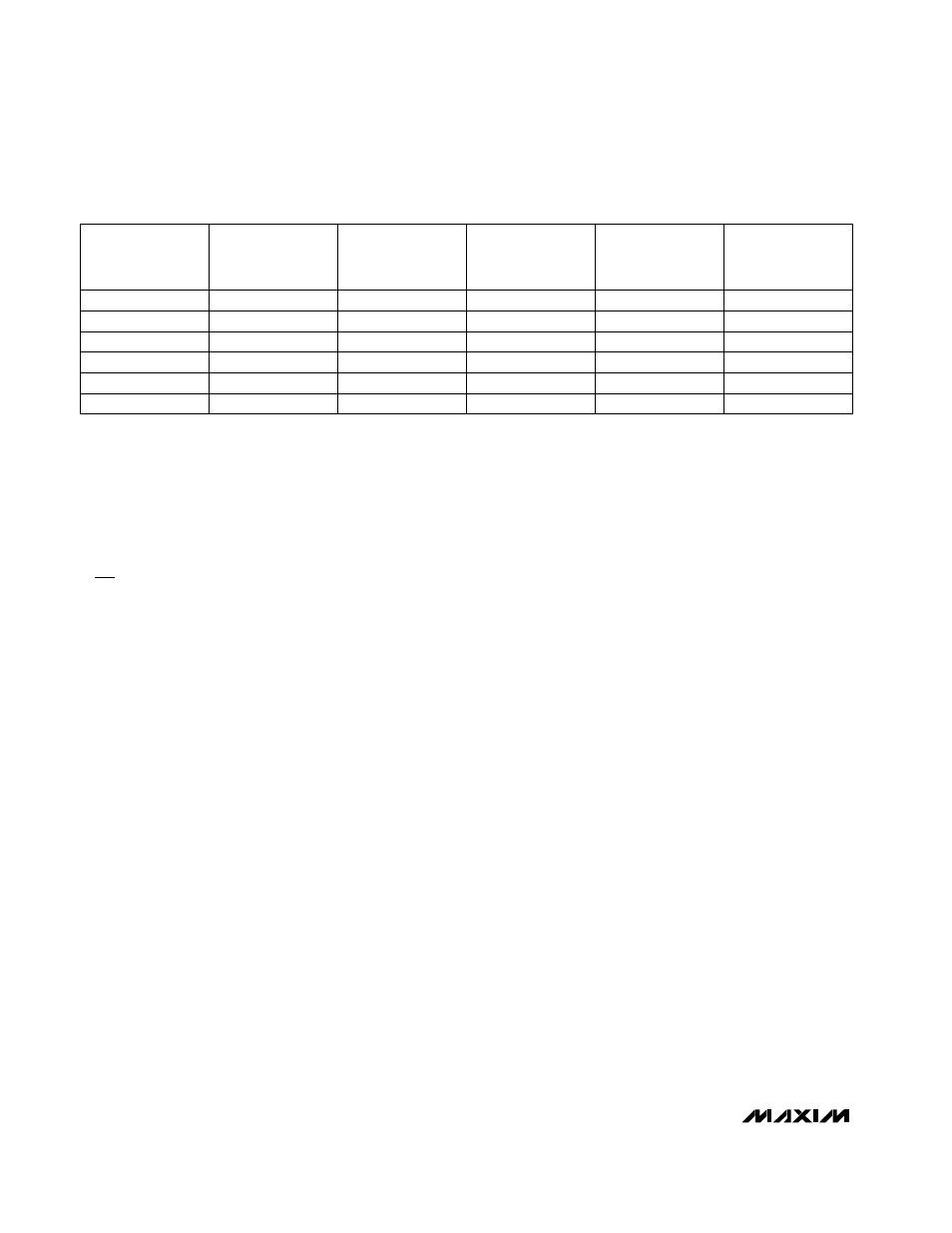
Table 4 shows how the choice of reference-buffer com-
pensation and power-down mode affects both power-up
REFERENCE
BUFFER
REFERENCE-
BUFFER
COMPENSATION
MODE
VREF
CAPACITOR
(µF)
POWER-DOWN
MODE
POWER-UP
DELAY
(µs)
MAXIMUM
SAMPLING RATE
(ksps)
Enabled
Internal
—
Fast
5
26
Enabled
Internal
—
Full
300
26
Enabled
External
4.7
Fast
See Figure 14c
133
Enabled
External
4.7
Full
See Figure 14c
133
Disabled
—
—
Fast
2
133
Disabled
—
—
Full
2
133
Table 4. Typical Power-Up Delay Times