Clock modes – Rainbow Electronics MAX149 User Manual
Page 11
MAX148/MAX149
+2.7V to +5.25V, Low-Power, 8-Channel,
Serial 10-Bit ADCs
______________________________________________________________________________________
11
Simple Software Interface
Make sure the CPU’s serial interface runs in master
mode so the CPU generates the serial clock. Choose a
clock frequency from 100kHz to 2MHz.
1) Set up the control byte for external clock mode and
call it TB1. TB1 should be of the format: 1XXXXX11
binary, where the Xs denote the particular channel
and conversion mode selected.
2) Use a general-purpose I/O line on the CPU to pull
CS low.
3) Transmit TB1 and, simultaneously, receive a byte
and call it RB1. Ignore RB1.
4) Transmit a byte of all zeros ($00 hex) and, simulta-
neously, receive byte RB2.
5) Transmit a byte of all zeros ($00 hex) and, simulta-
neously, receive byte RB3.
6) Pull CS high.
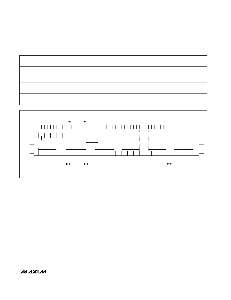
Figure 6 shows the timing for this sequence. Bytes RB2
and RB3 contain the result of the conversion, padded
with one leading zero, two sub-LSB bits, and three trail-
ing zeros. The total conversion time is a function of the
serial-clock frequency and the amount of idle time
between 8-bit transfers. To avoid excessive T/H droop,
make sure the total conversion time does not exceed
120µs.
Digital Output
In unipolar input mode, the output is straight binary
(Figure 17). For bipolar input mode, the output is twos
complement (Figure 18). Data is clocked out at the
falling edge of SCLK in MSB-first format.
Clock Modes
The MAX148/MAX149 may use either an external
serial clock or the internal clock to perform the succes-
sive-approximation conversion. In both clock modes,
the external clock shifts data in and out of the
SSTRB
CS
SCLK
DIN
DOUT
1
4
8
12
16
20
24
START
SEL2 SEL1 SEL0
UNI/
BIP
SGL/
DIF
PD1
PD0
B9
MSB
B8
B7
B6
B5
B4
B3
B2
B1
S0
S1
B0
LSB
ACQUISITION
(f
SCLK
= 2MHz)
IDLE
FILLED WITH
ZEROS
IDLE
CONVERSION
t
ACQ
A/D STATE
RB1
RB2
RB3
1.5
µ
s
Figure 6. 24-Clock External Clock Mode Conversion Timing (MICROWIRE and SPI-Compatible, QSPI-Compatible with f
SCLK
≤
2MHz)
SEL2
SEL1
SEL0
CH0
CH1
CH2
CH3
CH4
CH5
CH6
CH7
0
0
0
+
–
0
0
1
+
–
0
1
0
+
–
0
1
1
+
–
1
0
0
–
+
1
0
1
–
+
1
1
0
–
+
1
1
1
–
+
Table 3. Channel Selection in Differential Mode (SGL/
D
DIIF
F
= 0)