Rainbow Electronics MAX149 User Manual
Page 2
MAX148/MAX149
+2.7V to +5.25V, Low-Power, 8-Channel,
Serial 10-Bit ADCs
2
_______________________________________________________________________________________
ABSOLUTE MAXIMUM RATINGS
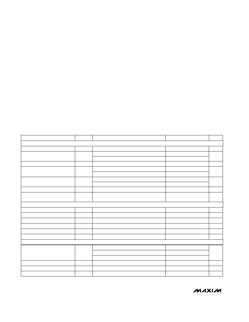
ELECTRICAL CHARACTERISTICS
V
DD
= +2.7V to +5.25V; COM = 0V; f
SCLK
= 2.0MHz; external clock (50% duty cycle); 15 clocks/conversion cycle (133ksps);
MAX149—4.7µF capacitor at VREF pin; MAX148—external reference, VREF = 2.500 V applied to VREF pin; T
A
= T
MIN
to T
MAX
; unless
otherwise noted.)
Stresses beyond those listed under “Absolute Maximum Ratings” may cause permanent damage to the device. These are stress ratings only, and functional
operation of the device at these or any other conditions beyond those indicated in the operational sections of the specifications is not implied. Exposure to
absolute maximum rating conditions for extended periods may affect device reliability.
V
DD
to AGND, DGND................................................. -0.3V to 6V
AGND to DGND ...................................................... -0.3V to 0.3V
CH0–CH7, COM to AGND, DGND ............ -0.3V to (V
DD
+ 0.3V)
VREF, REFADJ to AGND ........................... -0.3V to (V
DD
+ 0.3V)
Digital Inputs to DGND .............................................. -0.3V to 6V
Digital Outputs to DGND ........................... -0.3V to (V
DD
+ 0.3V)
Digital Output Sink Current .................................................25mA
Continuous Power Dissipation (T
A
= +70°C)
Plastic DIP (derate 11.11mW/°C above +70°C) ......... 889mW
SSOP (derate 8.00mW/°C above +70°C) ................... 640mW
CERDIP (derate 11.11mW/°C above +70°C) .............. 889mW
Operating Temperature Ranges
MAX148_C_P/MAX149_C_P .............................. 0°C to +70°C
MAX148_E_P/MAX149_E_P............................ -40°C to +85°C
MAX148_MJP/MAX149_MJP ........................ -55°C to +125°C
Storage Temperature Range ............................ -60°C to +150°C
Lead Temperature (soldering, 10sec) ............................ +300°C
µs
1.5
t
ACQ
Differential Nonlinearity
Track/Hold Acquisition Time
ns
30
Aperture Delay
6
µs
35
65
t
CONV
Conversion Time (Note 5)
5.5
7.5
ps
MHz
1.0
Full-Power Bandwidth
MHz
2.25
Small-Signal Bandwidth
dB
-75
Channel-to-Channel Crosstalk
dB
70
SFDR
Spurious-Free Dynamic Range
dB
-70
THD
Total Harmonic Distortion
dB
66
SINAD
Signal-to-Noise + Distortion Ratio
LSB
±0.05
Channel-to-Channel Offset
Matching
ppm/°C
±0.25
Gain Temperature Coefficient
±0.5
<50
Bits
10
Resolution
Gain Error (Note 3)
±1
Aperture Jitter
Offset Error
LSB
±1.0
INL
Relative Accuracy (Note 2)
LSB
±1
DNL
±0.15
±1
LSB
±0.15
±2
UNITS
MIN
TYP
MAX
SYMBOL
PARAMETER
External clock = 2MHz, 12 clocks/conversion
Internal clock, SHDN = V
DD
Internal clock, SHDN = FLOAT
MAX14_A
-3dB rolloff
65kHz, 2.500V
p-p
(Note 4)
Up to the 5th harmonic
MAX14_A
MAX14_B
No missing codes over temperature
MAX14_A
MAX14_B
CONDITIONS
LSB
±2
MAX14_B
DC ACCURACY
(Note 1)
DYNAMIC SPECIFICATIONS
(10kHz sine-wave input, 0V to 2.500Vp-p, 133ksps, 2.0MHz external clock, bipolar input mode)
CONVERSION RATE