Rainbow Electronics MAX149 User Manual
Page 21
High-Speed Digital Interfacing with QSPI
The MAX148/MAX149 can interface with QSPI using
the circuit in Figure 20 (f
SCLK
= 2.0MHz, CPOL = 0,
CPHA = 0). This QSPI circuit can be programmed to do a
conversion on each of the eight channels. The result is
stored in memory without taxing the CPU, since QSPI
incorporates its own microsequencer.
The MAX148/MAX149 are QSPI compatible up to the
maximum external clock frequency of 2MHz.
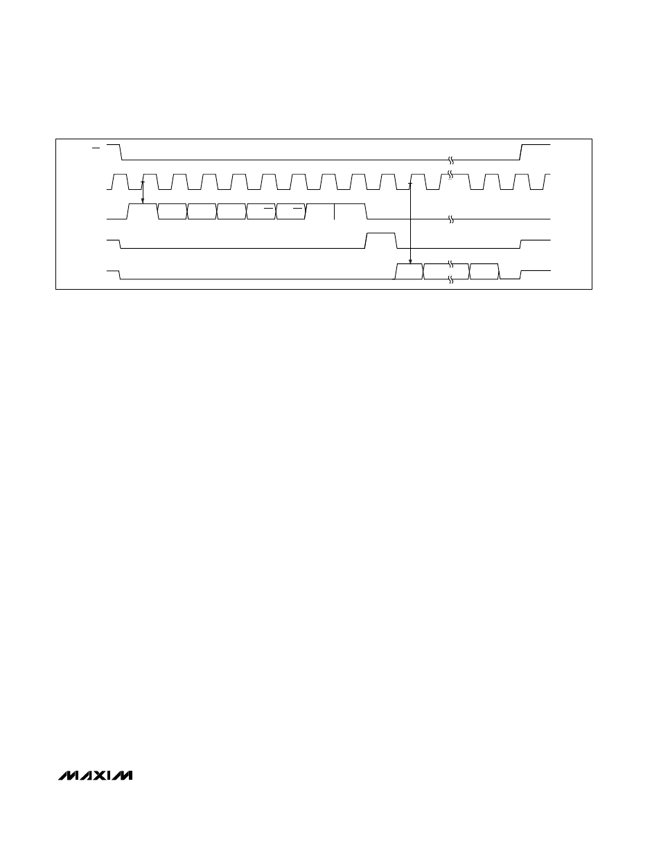
TMS320LC3x Interface
Figure 21 shows an application circuit to interface the
MAX148/MAX149 to the TMS320 in external clock mode.
The timing diagram for this interface circuit is shown in
Figure 22.
Use the following steps to initiate a conversion in the
MAX148/MAX149 and to read the results:
1) The TMS320 should be configured with CLKX
(transmit clock) as an active-high output clock and
CLKR (TMS320 receive clock) as an active-high
input clock. CLKX and CLKR on the TMS320 are
tied together with the MAX148/MAX149’s SCLK
input.
2) The MAX148/MAX149’s CS pin is driven low by the
TMS320’s XF_ I/O port to enable data to be clocked
into the MAX148/MAX149’s DIN.
3) An 8-bit word (1XXXXX11) should be written to the
MAX148/MAX149 to initiate a conversion and place
the device into external clock mode. Refer to Table
1 to select the proper XXXXX bit values for your
specific application.
4) The MAX148/MAX149’s SSTRB output is monitored
via the TMS320’s FSR input. A falling edge on the
SSTRB output indicates that the conversion is in
progress and data is ready to be received from the
MAX148/MAX149.
5) The TMS320 reads in one data bit on each of the
next 16 rising edges of SCLK. These data bits rep-
resent the 10 + 2-bit conversion result followed by
4 trailing bits, which should be ignored.
6) Pull CS high to disable the MAX148/MAX149 until
the next conversion is initiated.
MAX148/MAX149
+2.7V to +5.25V, Low-Power, 8-Channel,
Serial 10-Bit ADCs
______________________________________________________________________________________
21
CS
SCLK
DIN
SSTRB
DOUT
START
SEL2
SEL1
SEL0
UNI/BIP SGL/DIF
PD1
PD0
MSB
B8
S1
S0
HIGH
IMPEDANCE
HIGH
IMPEDANCE
Figure 22. TMS320 Serial-Interface Timing Diagram