Power-up reset, Atv2500b(q)(l) – Rainbow Electronics ATV2500BQL User Manual
Page 11
ATV2500B(Q)(L)
11
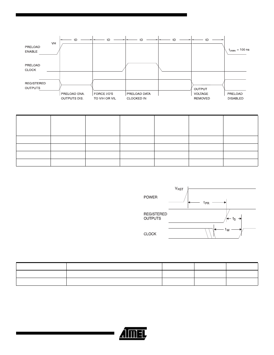
Power-up Reset
The registers in the ATV2500Bs are designed to reset dur-
ing power-up. At a point delayed slightly from V
CC
crossing
V
RST
, all registers will be reset to the low state. The output
state will depend on the polarity of the output buffer.
This feature is critical for state as nature of reset and the
uncertainty of how V
CC
actually rises in the system, the fol-
lowing conditions are required:
1.
The V
CC
rise must be monotonic,
2.
After reset occurs, all input and feedback setup
times must be met before driving the clock pin or
terms high, and
3.
The clock pin, and any signals from which clock
terms are derived, must remain stable during t
PR
.
.
Level Forced on
Odd I/O Pin
during
PRELOAD Cycle
Q Select Pin
State
Even/Odd Select
Even Q1 State
after Cycle
Even Q2 State
after Cycle
Odd Q1 State
after Cycle
Odd Q2 State
after Cycle
V
IH
/V
IL
Low
Low
High/Low
X
X
X
V
IH
/V
IL
High
Low
X
High/Low
X
X
V
IH
/V
IL
Low
High
X
X
High/Low
X
V
IH
/V
IL
High
High
X
X
X
High/Low
Parameter
Description
Typ
Max
Units
t
PR
Power-up Reset Time
600
1000
ns
V
RST
Power-up Reset Voltage
3.8
4.5
V