Ata8403, 4 application circuit – Rainbow Electronics ATA8401 User Manual
Page 6
6
4983A–IND–02/07
ATA8403
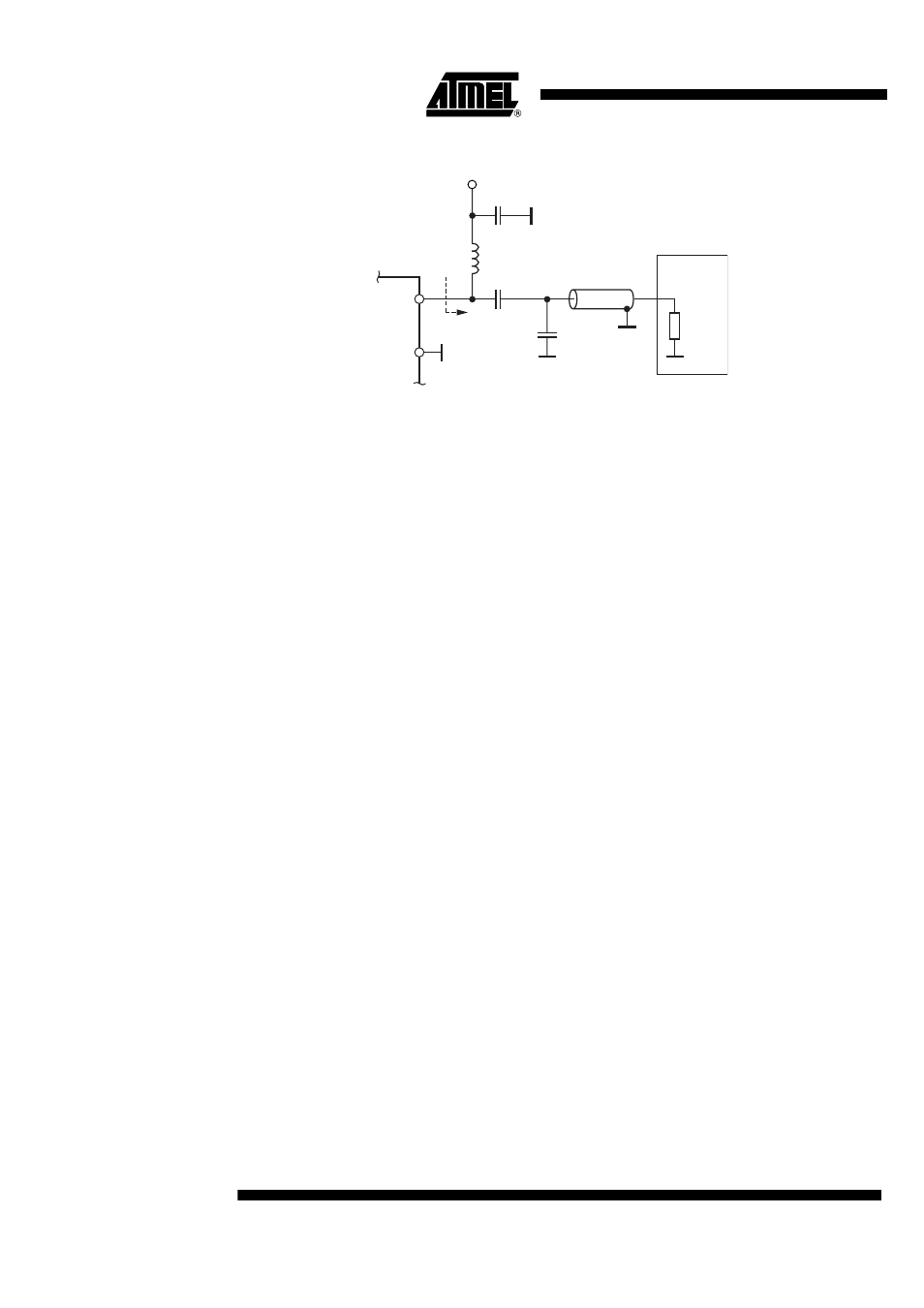
Figure 4-2.
Output Power Measurement
4.4
Application Circuit
A value of 68 nF/X7R is recommended for the supply-voltage blocking capacitor C
3
(see
). C
1
and C
2
are used to match the loop antenna to the
power amplifier where C
1
typically is 3.9 pF/NP0 and C
2
is 1 pF/NP0. For C
2
, two capacitors in
series should be used to achieve a better tolerance value and to have the possibility of realizing
the Z
Load,opt
using standard valued capacitors.
C
1
, together with the pins of ATA8403 and the PCB board wires, forms a series resonance loop
that suppresses the 1
st
harmonic. Therefore, the position of C
1
on the PCB is important. Nor-
mally the best suppression is achieved when C
1
is placed as close as possible to the pins ANT1
and ANT2.
The loop antenna should not exceed a width of 1.5 mm, otherwise the Q-factor of the loop
antenna is too high.
L
1
(
≈
50 nH to 100 nH) can be printed on PCB. C
4
should be selected so that the XTO runs on
the load resonance frequency of the crystal. Normally, a 15 pF load-capacitance crystal results
in a value of 12 pF.
1 nF
1.5 pF
2.7 pF
10 nH
C
1
C
2
C
3
L
1
V
S
R
in
ANT2
ANT1
Z
Lopt
Power
meter
50
Ω
Z = 50
Ω