Ata8403, 3 clk output – Rainbow Electronics ATA8401 User Manual
Page 5
5
4983A–IND–02/07
ATA8403
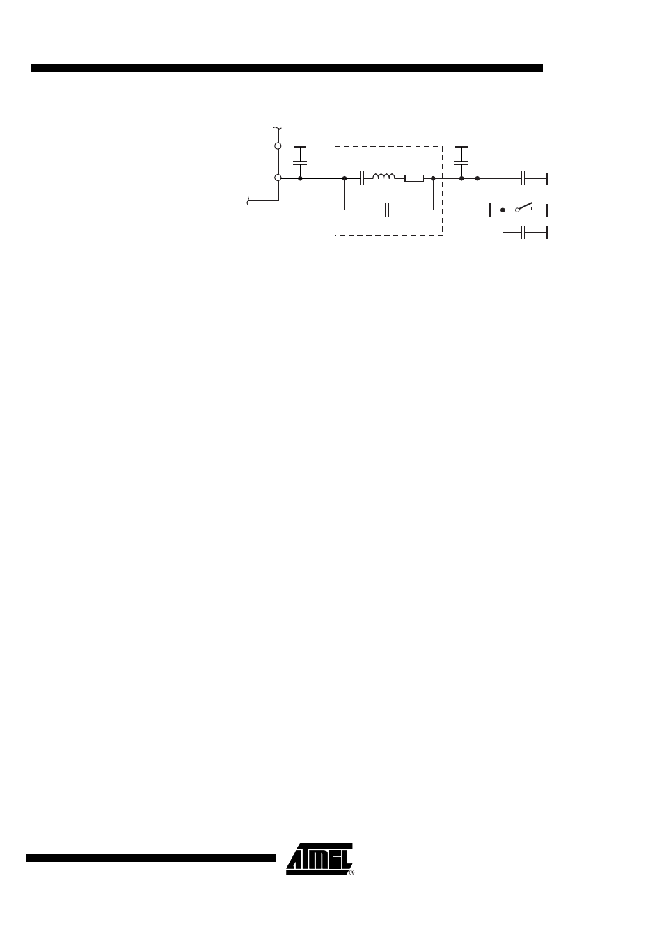
Figure 4-1.
Tolerances of Frequency Modulation
Using C
4
= 9.2 pF ±2%, C
5
= 6.8 pF ±5%, a switch port with C
Switch
= 3 pF ±10%, stray capaci-
tances on each side of the crystal of C
Stray1
= C
Stray2
= 1 pF ±10%, a parallel capacitance of the
crystal of C
0
= 3.2 pF ±10% and a crystal with C
M
= 13 fF ±10%, typically results in an FSK devi-
ation of ±21.5 kHz with worst case tolerances of ±16.8 kHz to ±28.0 kHz.
4.3
CLK Output
An output CLK signal is provided for a connected microcontroller. The delivered signal is CMOS
compatible if the load capacitance is lower than 10 pF.
4.3.1
Clock Pulse Take-over
The clock of the crystal oscillator can be used for clocking the microcontroller. A special feature
of Atmel
®
’s ATARx9x is that it starts with an integrated RC-oscillator to switch on the ATA8403
with ENABLE = H, and after 4 ms assumes the clock signal of the transmission IC, so that the
message can be sent with crystal accuracy.
4.3.2
Output Matching and Power Setting
The output power is set by the load impedance of the antenna. The maximum output power is
achieved with a load impedance of Z
Load,opt
= (166 + j226)
Ω
at 868.3 MHz. There must be a low
resistive path to V
S
to deliver the DC current.
The delivered current pulse of the power amplifier is 7.7 mA. The maximum output power is
delivered to a resistive load of 475
Ω
if the 0.53 pF output capacitance of the power amplifier is
compensated by the load impedance.
An optimum load impedance of:
Z
Load
= 475
Ω
|| j/(2
×
p
×
f
×
0.53 pF) = (166 + j226)
Ω
thus results in the maximum output power
of 5.5 dBm.
The load impedance is defined as the impedance seen from the ATA8403’s ANT1, ANT2 into
the matching network. Do not confuse this large signal load impedance with a small signal input
impedance delivered as input characteristic of RF amplifiers and measured from the application
into the IC instead of from the IC into the application for a power amplifier.
Less output power is achieved by lowering the real parallel part of 475
Ω
where the parallel imag-
inary part should be kept constant.
Output power measurement can be done with the circuit shown in
. Note
that the component values must be changed to compensate for the individual board parasitics
until the ATA8403 has the right load impedance Z
Load,opt
= (166 + j226)
Ω
at 868.3 MHz. Also the
damping of the cable used to measure the output power must be calibrated out.
R
S
L
M
C
4
C
M
V
S
XTAL
C
0
C
5
C
Switch
C
Stray1
C
Stray2