Applications information – Rainbow Electronics MAX8514 User Manual
Page 33

MAX8513/MAX8514
Wide-Input, High-Frequency, Triple-Output Supplies
with Voltage Monitor and Power-On Reset
______________________________________________________________________________________
33
Applications Information
PC Board Layout Guidelines
Careful PC board layout is critical to achieve low
switching losses and clean, stable operation. The
switching power stage requires particular attention.
Follow these guidelines for good PC board layout:
Place decoupling capacitors as close to the IC pins as
possible. Keep separate the power-ground plane (con-
nect to the sources of the low-side MOSFET, PGND,
and the output capacitor’s return). Connect the input
decoupling capacitors across the drain of the high-side
MOSFETs and the source of the low-side MOSFETs.
The signal-ground plane (connected to GND) is con-
nected to the rest of the circuit-ground return. The two
ground planes then connect together with a single con-
nection at the IC. Keep the high-current paths as short
as possible. Connect the drains of the MOSFETS to a
large copper area to help in cooling the devices, further
improving efficiency and long-term reliability.
1) Ensure all feedback connections are short and
direct. Place the feedback resistors as close to the
IC as possible.
2) Route high-speed switching nodes away from sen-
sitive analog areas (FB_, COMP, ILIM).
3) Ensure the current-sense paths for CSP and CSN
run parallel and close together to cancel any noise
pickup.
4) A reference PC board layout included in the
MAX8513 evaluation kit is also provided to further
aid layout.
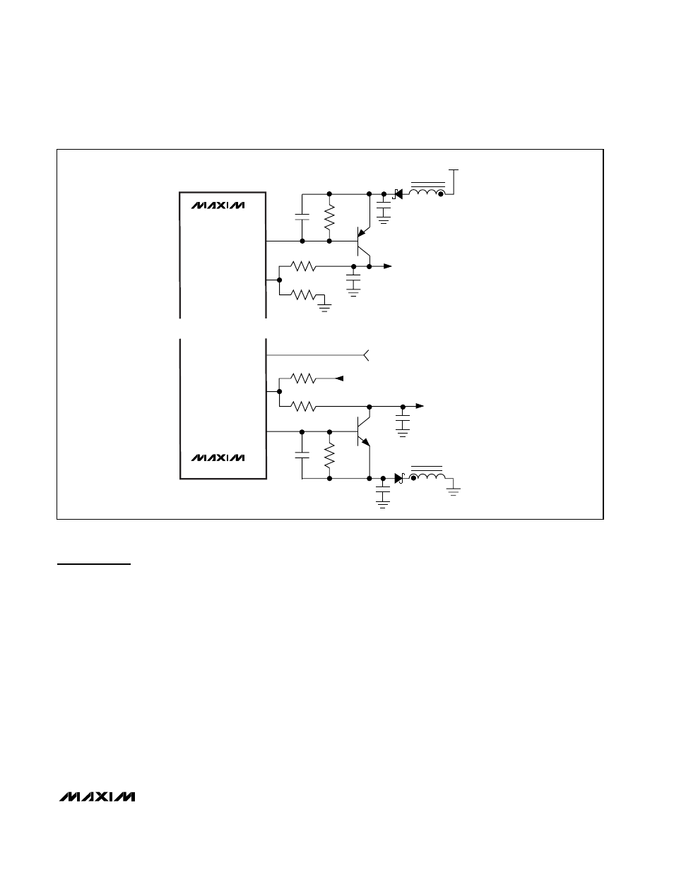
b) NEGATIVE OUTPUT VOLTAGE
V
OUT1
V
OUT1
V
OUT1
C7
V
OUT3N
Q4
C8
R12
CBE
R13
R14
DRV3P
a) POSITIVE OUTPUT VOLTAGE
FB3P
V
OUT3P
C7
Q4
C8
R12
C BE
R14
R13
FB3N
DRV3N
SUP3N
L1B
L1B
MAX8513
MAX8514
Figure 7. Base-Drive Noise Reduction
