Rainbow Electronics MAX8514 User Manual
Page 23
MAX8513/MAX8514
Wide-Input, High-Frequency, Triple-Output Supplies
with Voltage Monitor and Power-On Reset
______________________________________________________________________________________
23
When the output capacitance is comprised of parallel-
ing n number of identical capacitors whose values are
C
EACH
with ESR of R
ESR_EACH
, then:
Thus the resulting f
ZESR
is the same as that of each
capacitor.
The crossover frequency (f
C
), which is the frequency
when the closed-loop gain is equal to unity, should be
the smaller of 1/5th the switching frequency or 100kHz
(see the Switching-Frequency Setting section):
The loop-gain equation at the crossover frequency is:
where G
EA(fc)
is the error-amplifier gain at f
C
, and
G
MOD(
f
c)
is the power modular gain at f
C
.
The loop compensation is affected by the choice of out-
put-filter capacitor used, due to the position of its ESR
zero frequency with respect to the desired closed-loop
crossover frequency. Ceramic capacitors are used for
higher switching frequencies (above 750kHz) because
of low capacitance and low ESR; therefore, the ESR
zero frequency is higher than the closed-loop crossover
frequency. While electrolytic capacitors (e.g., tantalum,
solid polymer, oscon, etc.) are needed for lower switch-
ing frequencies, because of high capacitance and ESR,
the ESR zero frequency is typically lower than the
closed-loop crossover frequency. Thus the compensa-
tion design procedure is separated into two cases:
Case 1: Ceramic Output Capacitor (operating at
high switching frequencies, f
ZESR
> f
C
)
The modulator gain at f
C
is:
Since the crossover frequency is lower than the output
capacitors’ ESR zero frequency and higher than the LC
double-pole frequency, the error-amplifier gain must
have a +20dB/decade slope at f
C
. This +20dB/decade
slope of the error amplifier at crossover then adds to
the -40dB/decade slope of the LC double pole, and the
resultant compensated loop crosses over at the
desired -20dB/decade slope. The error amplifier has a
dominant pole at very low frequency (≈0Hz), and two
separate zeros at:
and poles at:
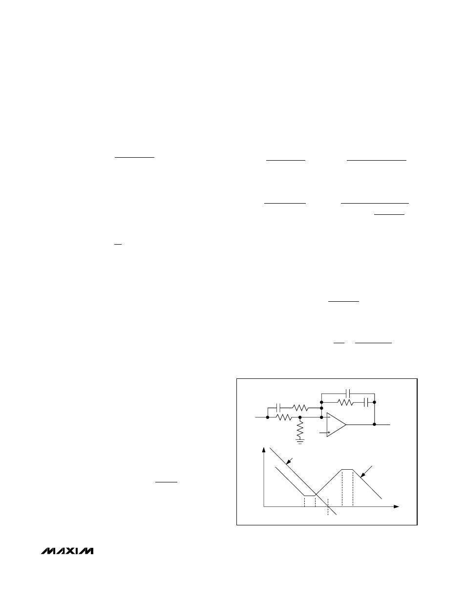
The error-amplifier equivalent circuit and its gain vs.
frequency plot are shown below in Figure 3.
In this case, f
Z2
and f
P1
are selected to have the convert-
ers’ closed-loop crossover frequency, f
C
, occur when the
error-amplifier gain has a +20dB/decade slope between
f
Z2
and f
P2
. The error-amplifier gain at f
C
is:
The gain of the error amplifier between f
Z1
and f
Z2
is:
G
G
f
f
f
f G
EA fZ fZ
EA fc
Z
C
Z
C MOD fc
(
)
( )
( )
1
2
2
2
-
=
=
G
G
EA fc
MOD fc
( )
( )
=
1
f
R
C
and f
R
C
C
C
C
P
P
2
3
1
2
4
11
1
2
3
5
12
5
12
=
Ч
Ч
=
Ч
Ч
Ч
+
π
π
f
R
C
and f
R
R
C
Z
Z
1
2
1
2
3
5
1
2
1
4
11
=
Ч
Ч
=
Ч
+
(
)
Ч
π
π
G
G
f
f
MOD fc
MOD DC
PMOD
C
( )
(
)
=
2
G
G
EA fc
MOD fc
( )
( )
= 1
f
f
or
kHz
C
S
≤
5
100
C
n
C
and
R
R
n
OUT
EACH
ESR
ESR EACH
_
=
×
=
Figure 3. Case 1: Error-Amplifier Compensation Circuit (Closed-
Loop and Error-Amplifier Gain Plot)
REF
R1
R3
R4
C12
C5
C11
COMP
R2
EA
V
OUT1
GAIN
(dB)
FREQUENCY
f
P3
f
P2
f
Z1
f
Z2
f
C
CLOSED-LOOP GAIN
EA GAIN