Rainbow Electronics MAX8514 User Manual
Page 25
MAX8513/MAX8514
Wide-Input, High-Frequency, Triple-Output Supplies
with Voltage Monitor and Power-On Reset
______________________________________________________________________________________
25
Use 6.8kΩ.
Use 4.7nF.
Use 620Ω.
Use 680pF.
Pick f
P3
= 700kHz, which is the midpoint between f
ZESR
and 1/2 the switching frequency.
Use 33pF.
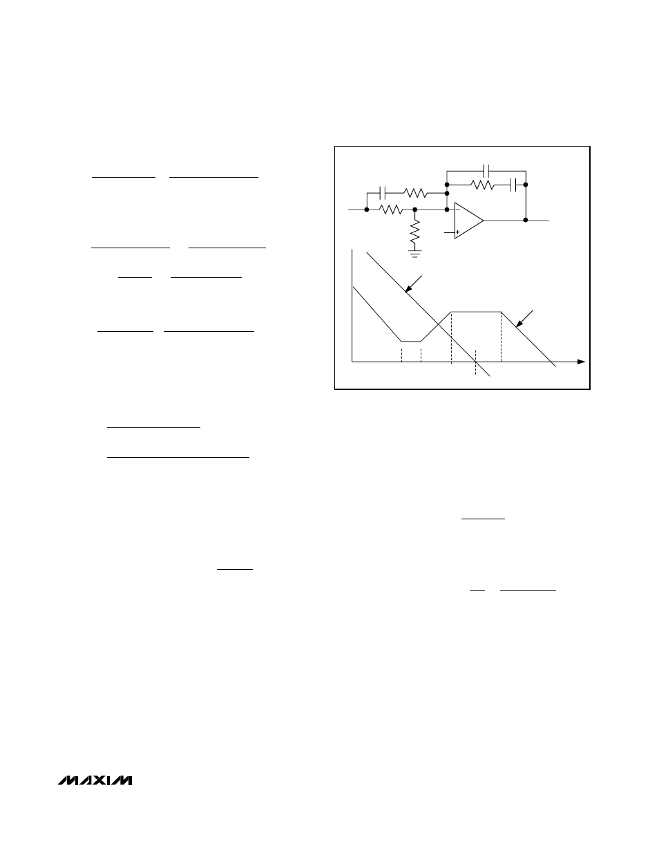
Case 2: Electrolytic Output Capacitor (operating at
lower switching frequencies, f
ZESR
< f
C
)
The modulator gain at f
C
is:
The output capacitor’s ESR zero frequency is higher
than the LC double-pole frequency but lower than the
closed-loop crossover frequency. Here the modulator
already has a -20dB/decade slope; therefore, the error-
amplifier gain must have a 0dB/decade slope at f
C
, so
the loop crosses over at the desired -20dB/decade
slope. The error-amplifier circuit configuration is the
same as Case 1; however, the closed-loop crossover
frequency is now between f
P2
and f
P3
, as illustrated in
Figure 4.
The equations that define the error amplifier’s poles
and zeroes (f
Z1
, f
Z2
, f
P2
, and f
P3
) are the same as for
Case 1. However, f
P2
is now lower than the closed-loop
crossover frequency.
The error-amplifier gain at f
C
is:
And the gain of the error amplifier between f
Z1
and
f
Z2
is:
Due to the underdamped (Q > 1) nature of the output LC
double pole, the error-amplifier zero frequencies must be
set less than the LC double-pole frequency to provide
adequate phase boost. Set the first zero of the error
amplifier, f
Z1
, at 1/4th the LC double-pole frequency. Set
the second zero, f
Z2
, at the LC double-pole frequency.
Set the second pole, f
P2
, at f
ZESR
.
G
G
f
f
f
f G
EA fZ
fZ
EA fc
Z
P
Z
P
MOD fc
(
)
( )
( )
1
2
2
2
2
2
−
=
=
G
G
EA fc
MOD fc
( )
( )
=
1
G
G
f
f
f
MOD fc
MOD DC
PMOD
ZESR C
( )
(
)
=
2
C
C
C
R
f
nF
nF
k
kHz
pF
P
12
5
2
5
3
4 7
2
4 7
6 8
700
33 7
3
=
Ч
Ч
Ч
=
Ч
Ч
Ч
=
(
)
.
(
.
.
)
.
π
π
-1
-1
Ω
C
R
f
kHz
pF
P
11
1
2
4
1
2
620
423
607
2
=
Ч
Ч
=
Ч
Ч
=
π
π
Ω
R
R
f
f
G
k
kHz
kHz
R
R
R
R
R
k
k
I
PMOD
P
EA fZ fZ
I
I
.
.
.
.
.
(
)
=
Ч
Ч
=
Ч
Ч
=
=
Ч
=
Ч
=
3
6 8
17 4
423
0 479
583
4
1
1
13 3
583
13 3
583
609
2
1
2
-
-
-
Ω
Ω
Ω
Ω
Ω
Ω
Ω
C
R
f
k
kHz
nF
PMOD
5
2
3
2
6 8
17 4
5 38
.
.
.
=
Ч
Ч
=
Ч
Ч
=
π
π
Ω
Figure 4. Case 2: Error-Amplifier Compensation Circuit (Closed-
Loop and Error-Amplifier Gain Plot)
V
REF
R1
R3
R4
C12
C5
C11
V
COMP
R2
EA
V
OUT1
GAIN
(dB)
FREQUENCY
f
P3
f
P2
f
Z1
f
Z2
f
C
CLOSED-LOOP GAIN
EA GAIN