30v n-channel power mosfet, Electrical specifications – Rainbow Electronics TSM15N03PQ33 User Manual
Page 2
TSM15N03PQ33
30V N-Channel Power MOSFET
2/4
Version: A12
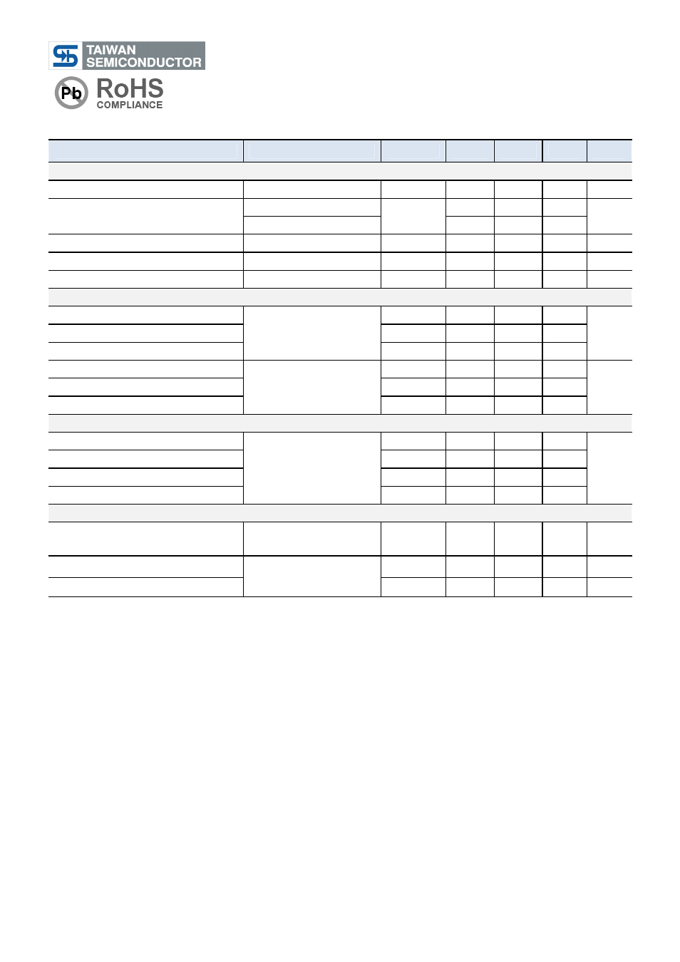
Electrical Specifications
(Ta = 25
o
C unless otherwise noted)
Parameter
Conditions
Symbol
Min
Typ
Max
Unit
Static
Drain-Source Breakdown Voltage
V
GS
= 0V, I
D
= 250uA
BV
DSS
30
--
--
V
Drain-Source On-State Resistance
V
GS
= 10V, I
D
= 7.8A
R
DS(ON)
--
9
12
m
Ω
V
GS
= 4.5V, I
D
= 7A
--
13
17
Gate Threshold Voltage
V
DS
= V
GS
, I
D
= 250uA
V
GS(TH)
1.2
--
2.5
V
Zero Gate Voltage Drain Current
V
DS
= 24V, V
GS
= 0V
I
DSS
--
--
1
uA
Gate Body Leakage
V
GS
= ±20V, V
DS
= 0V
I
GSS
--
--
±100
nA
Dynamic
Total Gate Charge
V
DS
= 15V, I
D
= 7.8A,
V
GS
= 4.5V
Q
g
--
3.6
--
nC
Gate-Source Charge
Q
gs
--
1.2
--
Gate-Drain Charge
Q
gd
--
1
--
Input Capacitance
V
DS
= 15V, V
GS
= 0V,
f = 1.0MHz
C
iss
--
415
--
pF
Output Capacitance
C
oss
--
90
--
Reverse Transfer Capacitance
C
rss
--
38
--
Switching
Turn-On Delay Time
V
GS
= 4.5V, V
DS
= 15V,
R
G
= 1
Ω
t
d(on)
--
13
--
nS
Turn-On Rise Time
t
r
--
10
--
Turn-Off Delay Time
t
d(off)
--
11
--
Turn-Off Fall Time
t
f
--
8
--
Drain-Source Diode Characteristics and Maximum Rating
Drain-Source Diode Forward
Voltage
V
GS
=0V, I
S
=6.3A
V
SD
--
0.8
1.3
V
Reverse Recovery Time
I
S
= 6.3A, T
J
=25
o
C
dI/dt = 100A/us
t
fr
--
15
--
nS
Reverse Recovery Charge
Q
fr
--
7
--
nC
Notes:
1. Pulse Test: Pulse Width
≤
300
µ
s, Duty Cycle
≤
2%.
2. R
θ
JA
is the sum of the junction-to-case and case-to-ambient thermal resistance where the case thermal
reference is defined as the solder mounting surface of the drain pins. R
θ
JC
is guaranteed by design while R
θ
CA
is determined by the user's board design. R
θ
JA
shown below for single device operation on FR-4 in still air
3. The maximum current rating is limited by package.