Th7899m – Rainbow Electronics TH7899M User Manual
Page 8
8
TH7899M
2201A–IMAGE–02/02
Table 2. Drive Clock Characteristics
Parameter
Min.
Typ.
Max.
Notes
Φ
P1,2,4
Low
High
-11V
+3.5V
-9V
+4V
-8.5V
+4.5V
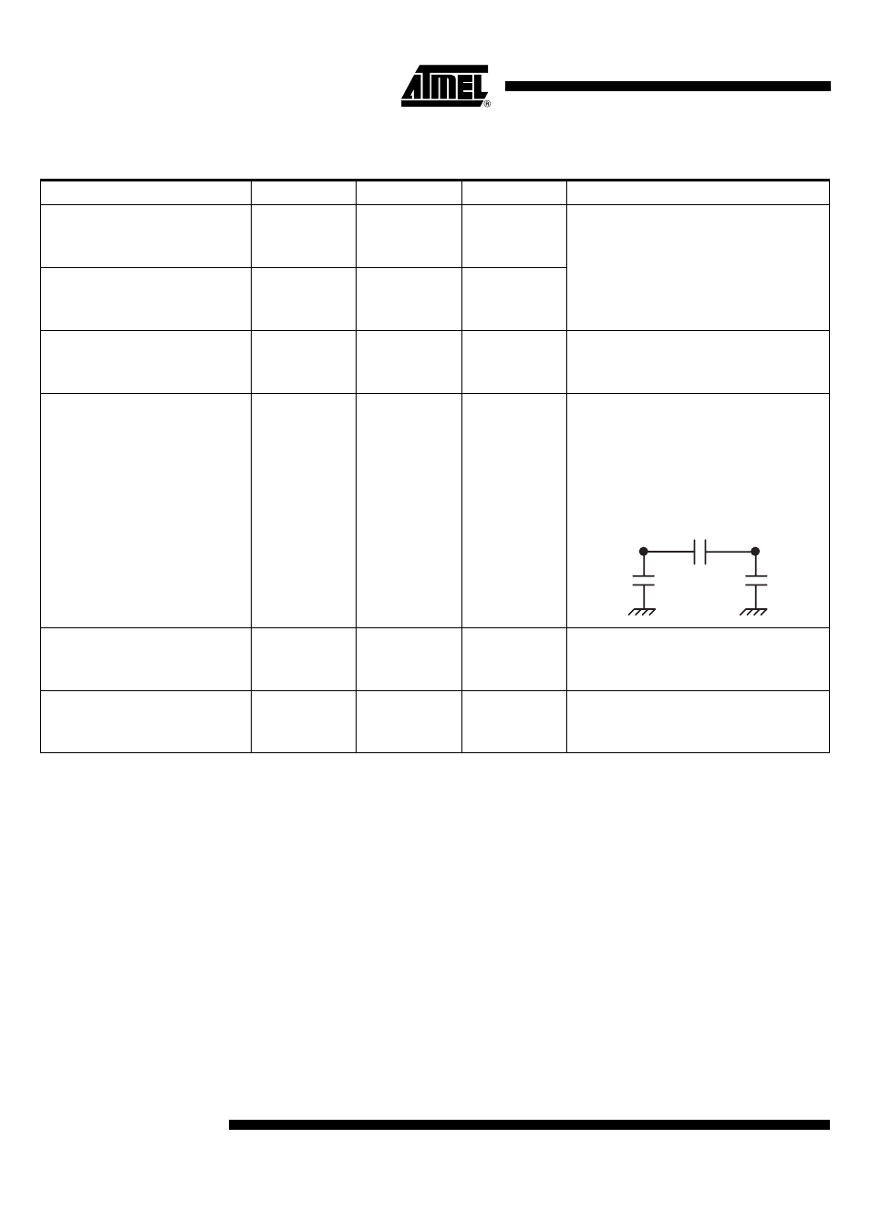
For each A,B,C and D zones, the
capacitances to drive are:
C
Φ
P1 = C
Φ
P3 = 10 nF
C
Φ
P2 = C
Φ
P4 = 13 nF
Φ
P3
Low
High
-11V
0V
-9V
0.3V
-8.5V
0.6V
Φ
T
(A and B)
Low
High
-11V
+3.5V
-9V
+4V
-8.5V
+5V
C
Φ
TA = C
Φ
TB < 100 pF
Φ
L
Low
High
-2.5V
+5.5V
-3V
+6V
-3.5V
+6.5V
-8V for MPP mode (option)
+3V for MPP mode (option)
For each A and B readout register and
after having tied the different clocks in two
clocks
Φ
L1 and
Φ
L2 and in the non MPP
mode (in the MPP mode the
Φ
L clock
capacitances are roughly 30% higher)
Φ
S
(1 to 4)
Low
High
-2.5V
+5.5V
-3V
+6V
3.5V
+6.5V
-8V for MPP mode (option)
+3V for MPP mode (option)
For each summing gate: C
Φ
S < 50 pF
Φ
R
(1 to 4)
Low
High
0V
+9V
0.3V
+10V
0.6V
+11V
For each reset gate: C
Φ
R < 20 pF
400 pF
400 pF
100 pF
Φ
L1
Φ
L2