Outline drawing, Th7899m, Top view – Rainbow Electronics TH7899M User Manual
Page 22
22
TH7899M
2201A–IMAGE–02/02
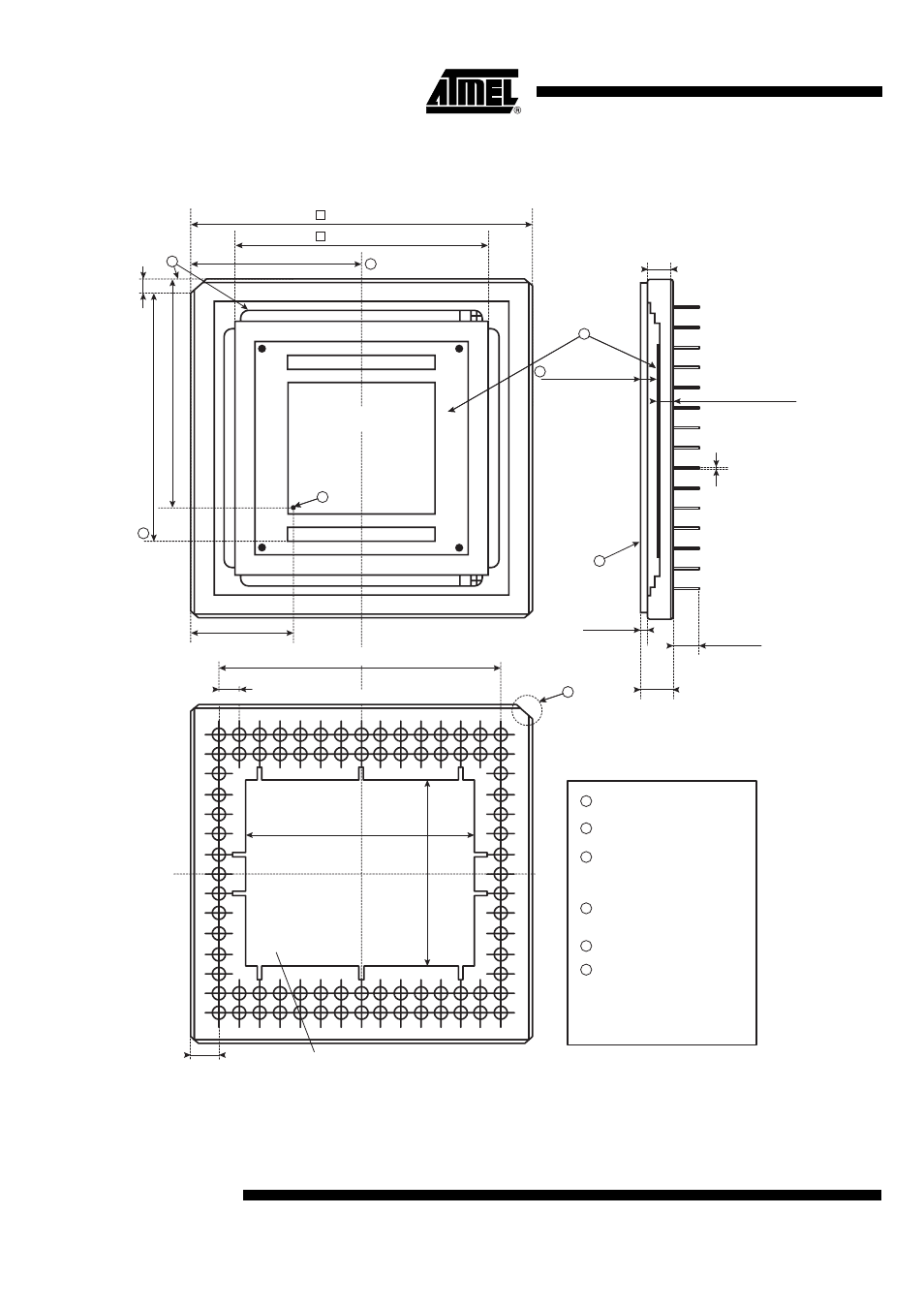
Outline Drawing
The chip center is located at package center.
A
B
C
D
E
F
G
H
J
K
L
M
N
P
R
2.97±0.25
25.00±0.25
30.00±0.30
2.54±0.13
2.00
X = 6.42±0.1
21.00
33.00±0.33
Ztop=2.07±0.25
Vos1
Vos2
Vos3
Vos4
Top view
35.56±0.20 (2.54 x 14)
1.5±0.1
4.57±0.25
Ø0.46±0.05
(82x)
4.77±0.45
3.17±0.30
Y=35.26±0.1
38.00
15 14 13 12 11 10 9
8
7
6
5
4
3
2 1
5
1
6
4
4
2
3
5
1
Glass window
2
Die and photosensitive area
3
Optical distance Z
top
between
external face of the window
and photosensitive area
4
Mechanical references/
die positionneing (first pixels)
5
Pin n˚ A1 index
6
Co-ordinates X,Y,Z of the first
active and photosensitive pixel
on VOS1 output.
Dimensions in mm
Metallic plane connected
to Vss pins (must be grounded on electronic board)
41.50±0.42
Zbot=2.70±0.23