Pin-out/pin designation, Th7899m – Rainbow Electronics TH7899M User Manual
Page 23
23
TH7899M
2201A–IMAGE–02/02
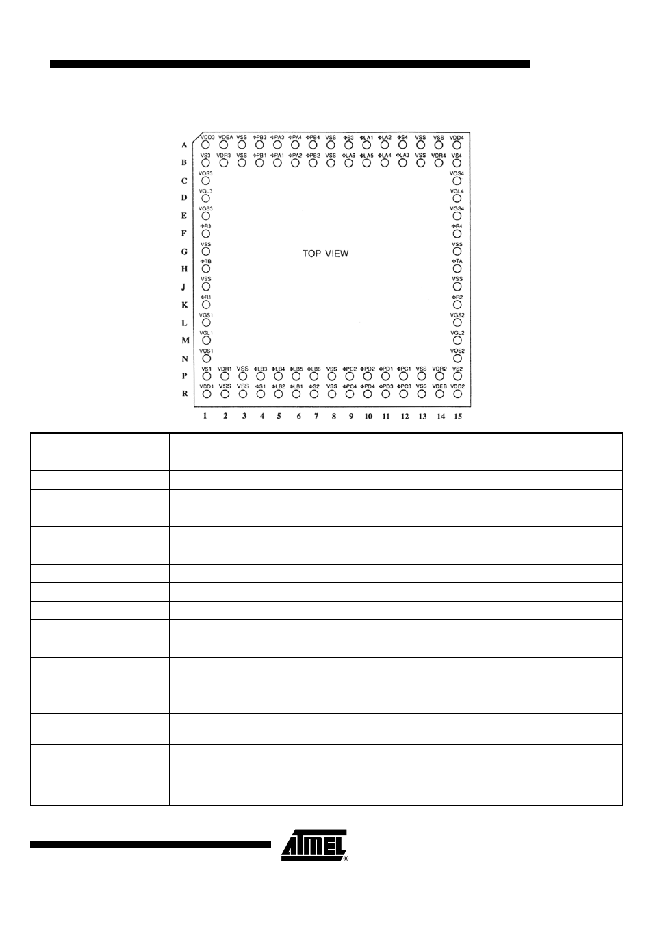
Pin-out/Pin Designation
Pin n°
Symbol
Designation
R6, R5, P4, P5, P6, P7
Φ
LB1,
Φ
LB2,
Φ
LB3,
Φ
LB4,
Φ
LB5,
Φ
LB6
B readout register clocks
A10, A11, B12, B11, B10, B9
Φ
LA1,
Φ
LA2,
Φ
LA3,
Φ
LA4,
Φ
LA5,
Φ
LA6
A readout register clocks
R4, R7, A9, A12
Φ
S1,
Φ
S@,
Φ
S3,
Φ
S4
Summing clocks of the output 1, 2, 3 and 4
M1, M15, D1, D15
VGL1, VGL2, VGL3, VGL4
Readout gate bias of the output 1, 2, 3 and 4
L1, L15, E1, E15
VGS1, VGS2, VGS3, VGS4
Output gate bias of the output 1, 2, 3 and 4
N1, N15, C1, C15
VOS1, VOS2, VOS3, VOS4
Output signal video 1, 2, 3 and 4
R1, R15, A1, A15
VDD1, VDD2, VDD3, VDD4
Output amplifier drain supply of the output 1, 2, 3 and 4
P1, P15, B1, B15
VS1, VS2, VS3, VS4
Output amplifier source bias of the output 1, 2, 3 and 4
K1, K15, F1, F15
Φ
R1,
Φ
R2,
Φ
R3,
Φ
R4
Reset clocks of the output 1, 2, 3 and 4
P2, P14, B2, B14
VDR1, VDR2, VDR3, VDR4
Reset bias of the output 1, 2, 3 and 4
B5, B6, A5, A6
Φ
PA1,
Φ
PA2,
Φ
PA3,
Φ
PA4
A image zone clocks
B4, B7, A4, A7
Φ
PB1,
Φ
PB2,
Φ
PB3,
Φ
PB4
B image zone clocks
P12, P9, R12, R9,
Φ
PC1,
Φ
PC2,
Φ
PC3,
Φ
PC4
C image zone clocks
P11, P10, R11, R10
Φ
PD1,
Φ
PD2,
Φ
PD3,
Φ
PD4
D image zone clocks
H15, H1
Φ
TA,
Φ
TB
Transfer gate from the image zone to the readout
registers A and B respectively
A2, R14
VDEA, VDEB
Shield drain
A3, A8, A13, A14, B3, B8,
B13, G1, G15, J1, J15, P3,
P8, P13, R2, R3, R8, R13
VSS
Substrate bias