Rainbow Electronics MAX8742 User Manual
Page 26
MAX8741/
M
AX8742
500kHz Multi-Output Power-Supply Controllers
with High Impedance in Shutdown
26
______________________________________________________________________________________
scale down the voltage. Use the maximum inductance
and minimum DCR to get the maximum possible induc-
tor time constant. Select R
S
and C
S
so that the maxi-
mum sense-network time constant is equal to or greater
than the maximum inductor time constant.
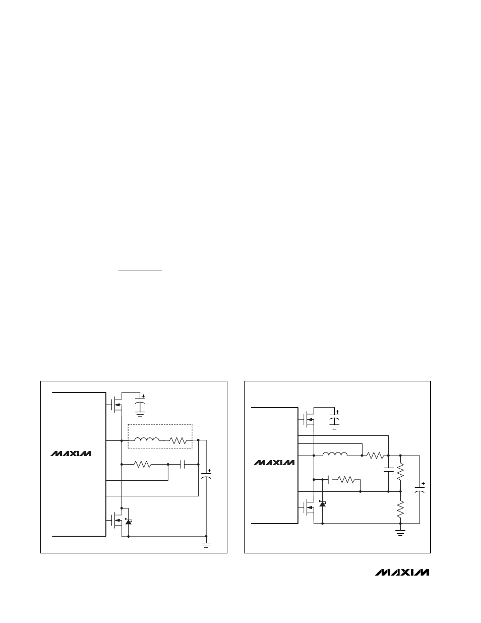
Reduced Output-Capacitance Application
In applications where higher output ripple is accept-
able, lower output capacitance or higher ESR output
capacitors can be used. In such cases, cycle-by-cycle
stability is maintained by adding feed-forward compen-
sation to offset for the increased output ESR. Figure 8
shows the addition of the feed-forward compensation
circuit. C
FB
provides noise filtering, R
FF
is the feed-for-
ward resistor, and C
LX
provides DC blocking. Use
100pF for C
FB
and C
LX
. Select R
FF
according to the
equation below:
Set the value for R
FF
close to the calculation. Do not
make R
FF
too small as that introduces too much feed-
forward, possibly causing an overvoltage to be seen at
the feedback pin, and changing the mode of operation
to a voltage mode.
PC Board Layout Considerations
Good PC board layout is required in order to achieve
specified noise, efficiency, and stability performance.
The PC board layout artist must be given explicit
instructions, preferably a pencil sketch showing the
placement of power-switching components and high-
current routing. A ground plane is essential for optimum
performance. In most applications, the circuit is located
on a multilayer board, and full use of the four or more
copper layers is recommended. Use the top layer for
high-current connections, the bottom layer for quiet
connections (REF, SS, GND), and the inner layers for
an uninterrupted ground plane. Use the following step-
by-step guide:
1) Place the high-power components (Figure 1, C1, C3,
C4, Q1, Q2, L1, and R1) first, with their grounds
adjacent:
• Priority 1: Minimize current-sense resistor trace
lengths and ensure accurate current sensing with
Kelvin connections (Figure 9).
• Priority 2: Minimize ground trace lengths in the
high-current paths (discussed below).
• Priority 3: Minimize other trace lengths in the
high-current paths.
a) Use >5mm-wide traces
b) CIN to high-side MOSFET drain: 10mm max
length
c) Rectifier diode cathode to low-side MOSFET:
5mm max length
R
R
L
f
ESR
FF
≤
Ч
Ч
Ч
4
3
L
DL_
DH_
LX_
MAX8741
MAX8742
CSH_
CSL_
INDUCTOR
R
L
V
OUT
V
IN
C
IN
C
OUT
C
S
R
S
Figure 7. Lossless Inductor Current Sensing
R3
R4
FB_
L
C
IN
DL_
DH_
LX_
MAX8741
MAX8742
CSH_
CSL_
V
IN
C
LX
R
FF
C
FB
R
SENSE
V
OUT
C
OUT
Figure 8. Adding Feed-Forward Compensation