Table 3. skip pwm table – Rainbow Electronics MAX8742 User Manual
Page 16
MAX8741/
M
AX8742
500kHz Multi-Output Power-Supply Controllers
with High Impedance in Shutdown
16
______________________________________________________________________________________
The output filter capacitors (Figure 1, C1 and C2) set a
dominant pole in the feedback loop that must roll off the
loop gain to unity before encountering the zero intro-
duced by the output capacitor’s parasitic resistance
(ESR) (see the Design Procedure section). A 50kHz
pole-zero cancellation filter provides additional rolloff
above the unity-gain crossover. This internal 50kHz
lowpass compensation filter cancels the zero due to fil-
ter-capacitor ESR. The 50kHz filter is included in the
loop in both fixed-output and adjustable-output modes.
Synchronous Rectifier Driver (DL)
Synchronous rectification reduces conduction losses in
the rectifier by shunting the normal Schottky catch
diode with a low-resistance MOSFET switch. Also, the
synchronous rectifier ensures proper startup of the
boost gate-driver circuit.
If the circuit is operating in continuous-conduction
mode, the DL drive waveform is the complement of the
DH high-side drive waveform (with controlled dead time
to prevent cross-conduction or “shoot-through”). In dis-
continuous (light-load) mode, the synchronous switch is
turned off as the inductor current falls through zero. The
synchronous rectifier works under all operating condi-
tions, including idle mode.
The SECFB signal further controls the synchronous switch
timing in order to improve multiple-output cross-regulation
(see the Secondary Feedback Regulation Loop section).
Internal V
L
and REF Supplies
An internal regulator produces the 5V supply (V
L
) that
powers the PWM controller, logic, reference, and other
blocks within the IC. This 5V low-dropout linear regula-
tor supplies up to 25mA for external loads, with a
reserve of 25mA for supplying gate-drive power.
Bypass V
L
to GND with 4.7µF.
Important:
Ensure that V
L
does not exceed 6V.
Measure V
L
with the main output fully loaded. If it is
pumped above 5.5V, either excessive boost-diode
capacitance or excessive ripple at V+ is the probable
cause. Use only small-signal diodes for the boost cir-
cuit (10mA to 100mA Schottky or 1N4148 are pre-
ferred), and bypass V+ to PGND with 4.7µF directly at
the package pins.
Table 3.
SKIP
PWM Table
SKIP
LOAD CURRENT
MODE
DESCRIPTION
Low
Light
Idle
Pulse skipping, supply current = 250µA at V
IN
=12V, discontinuous inductor
Low
Heavy
PWM
Constant-frequency PWM continuous-inductor current
High
Light
PWM
Constant-frequency PWM continuous-inductor current
High
Heavy
PWM
Constant-frequency PWM continuous-inductor current
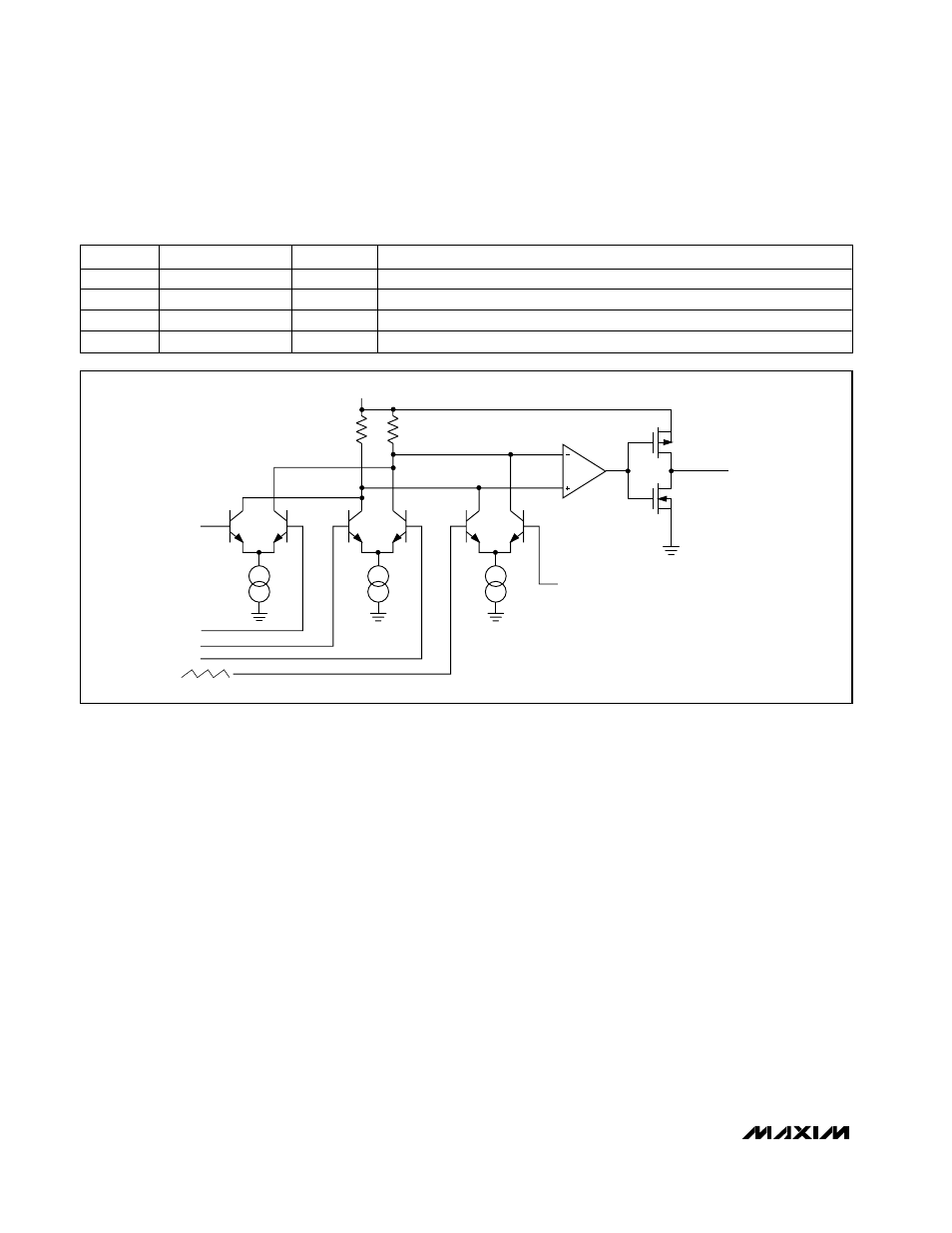
FB_
REF
CSH_
CSL_
SLOPE COMPENSATION
V
L
I1
R1
R2
TO PWM
LOGIC
OUTPUT DRIVER
UNCOMPENSATED
HIGH-SPEED
LEVEL TRANSLATOR
AND BUFFER
I2
I3
V
BIAS
Figure 4. Main PWM Comparator Block Diagram