Rainbow Electronics MAX9796 User Manual
Page 25
Single-Ended Input
The MAX9796 can be configured as a single-ended
input amplifier by appropriately configuring the Input
Control Register (see Tables 5a and 5b).
DC-Coupled Input
The input amplifier can accept DC-coupled inputs that
are biased to the amplifier’s bias voltage. DC-coupling
eliminates the input-coupling capacitors; reducing com-
ponent count to potentially six external components (see
the
Typical Application Circuit
). However, the highpass
filtering effect of the capacitors is lost, allowing low-fre-
quency signals to feed through to the load.
Unused Inputs
Connect any unused input directly to V
BIAS
. This saves
input capacitors on unused inputs and provides the
highest noise immunity on the input.
Component Selection
Input Filter
An input capacitor (C
IN
) in conjunction with the input
impedance of the MAX9796 forms a highpass filter that
removes the DC bias from the incoming signal. The AC-
coupling capacitor allows the amplifier to automatically
bias the signal to an optimum DC level. Assuming zero
source impedance, the -3dB point of the highpass filter
is given by:
Choose C
IN
so that f
-3dB
is well below the lowest fre-
quency of interest. Use capacitors whose dielectrics
have low-voltage coefficients, such as tantalum or alu-
minum electrolytic. Capacitors with high-voltage coeffi-
cients, such as ceramics, may result in increased
distortion at low frequencies.
Other considerations when designing the input filter
include the constraints of the overall system and the
actual frequency band of interest. Although high-fidelity
audio calls for a flat-gain response between 20Hz and
20kHz, portable voice-reproduction devices, such as
cell phones and two-way radios, need only concentrate
on the frequency range of the spoken human voice
(typically 300Hz to 3.5kHz). In addition, speakers used
in portable devices typically have a poor response
below 300Hz. Taking these two factors into considera-
tion, the input filter may not need to be designed for a
20Hz to 20kHz response, saving both board space and
cost due to the use of smaller capacitors.
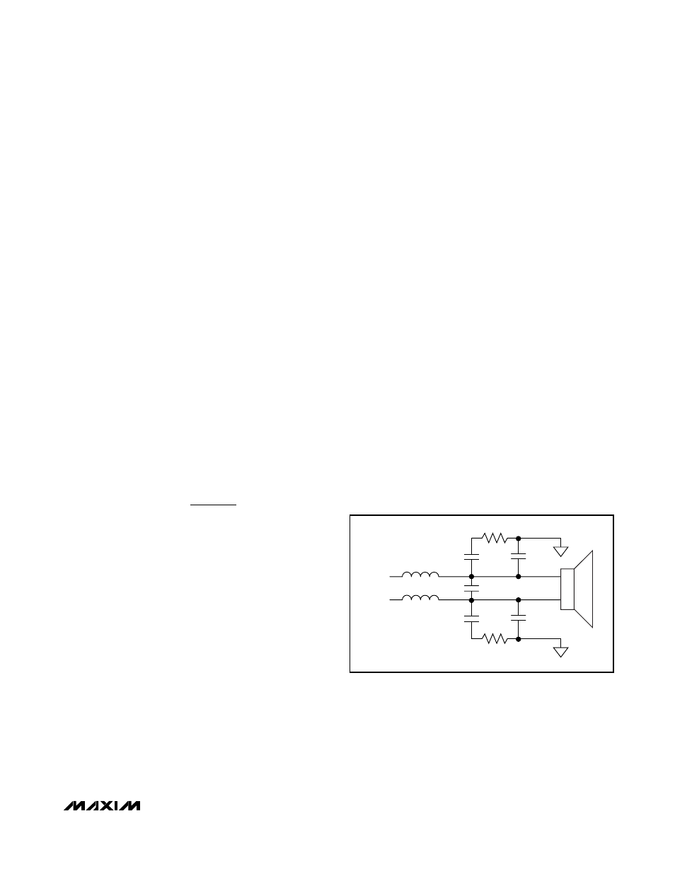
Class D Output Filter
The MAX9796 does not require a Class D output filter.
The device passes EN55022B emissions standards
with 152mm of unshielded speaker cables. However,
output filtering can be used if a design is failing radiat-
ed emissions due to board layout or cable length, or
the circuit is near EMI-sensitive devices. Use a ferrite
bead filter when radiated frequencies above 10MHz
are of concern. Use an LC filter when radiated frequen-
cies below 10MHz are of concern, or when long leads
(>152mm) connect the amplifier to the speaker. Figure
11 shows optional speaker amplifier output filters.
External Component Selection
BIAS Capacitor
V
BIAS
is the output of the internally generated DC bias
voltage. The V
BIAS
bypass capacitor, C
VBIAS
improves
PSRR and THD+N by reducing power supply and other
noise sources at the common-mode bias node, and
also generates the clickless/popless, startup/shutdown
DC bias waveforms for the speaker amplifiers. Bypass
V
BIAS
with a 1µF capacitor to GND.
f
R C
dB
IN IN
−
=
3
1
2
π
MAX9796
2.3W, High-Power Class D Audio Subsystem
with DirectDrive Headphone Amplifiers
______________________________________________________________________________________
25
OUT_+
OUT_-
33
µH
33
µH
0.47
µF
0.033
µF
0.1
µF
22
Ω
22
Ω
0.033
µF
0.1
µF
Figure 11. Speaker Amplifier Output Filter