Pin description – Rainbow Electronics MAX9796 User Manual
Page 12
MAX9796
2.3W, High-Power Class D Audio Subsystem
with DirectDrive Headphone Amplifiers
12
______________________________________________________________________________________
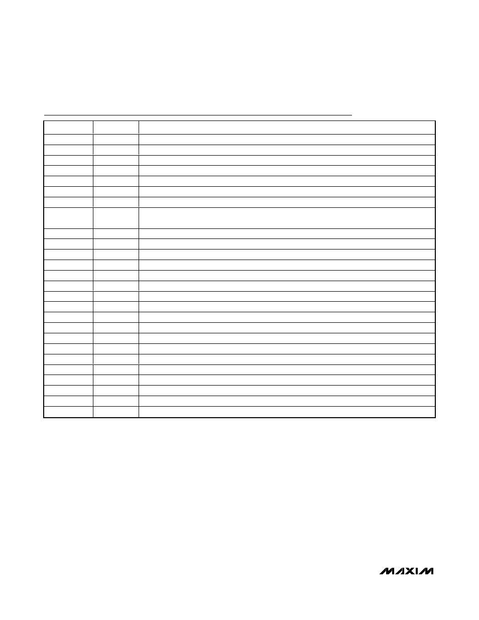
Pin Description
BUMP
NAME
FUNCTION
A1
CPV
DD
Charge-Pump Power Supply
A2
C1P
Charge-Pump Flying Capacitor Positive Terminal
A3
CPGND
Charge-Pump GND
A4
C1N
Charge-Pump Flying Capacitor Negative Terminal
A5
CPV
SS
Charge-Pump Output. Connect to V
SS
.
A6
HPL
Left Headphone Output
B1, F1, F5
PV
DD
Class D Power Supply
B2, E6
I.C.
Internal Connection. Leave unconnected. This pin is internally connected to the signal path. Do not
connect together or to any other pin.
B3
VBIAS
Common-Mode Bias
B4
INC1
Input C1. Left input or positive input (see Table 5a).
B5
V
SS
Headphone Amplifier Negative Power Supply. Connect to CPV
SS
.
B6
HPR
Right Headphone Output
C1, F4
OUT+
Positive Speaker Output
C2
SDA
Serial Data Input. Connect a 1k
Ω pullup resistor from SDA to V
DD
.
C5
INC2
Input C2. Right input or negative input (see Table 5a).
C6
OUTRx
Mono Receiver Output
D1, F3
PGND
Power Ground
D2
SCL
Serial Clock Input. Connect a 1k
Ω pullup resistor from SCL to V
DD
.
D5
INB2
Input B2. Right input or negative input (see Table 5a).
D6
V
DD
Analog Power Supply
E1, F2
OUT-
Negative Speaker Output
E2
SHDN
Active-Low Hardware Shutdown
E3
INA1
Input A1. Left input or positive input (see Table 5a).
E4
INA2
Input A2. Right input or negative input (see Table 5a).
E5
INB1
Input B1. Left input or positive input (see Table 5a).
F6
GND
Analog Ground