Rainbow Electronics MAX9796 User Manual
Page 2
MAX9796
2.3W, High-Power Class D Audio Subsystem
with DirectDrive Headphone Amplifiers
2
_______________________________________________________________________________________
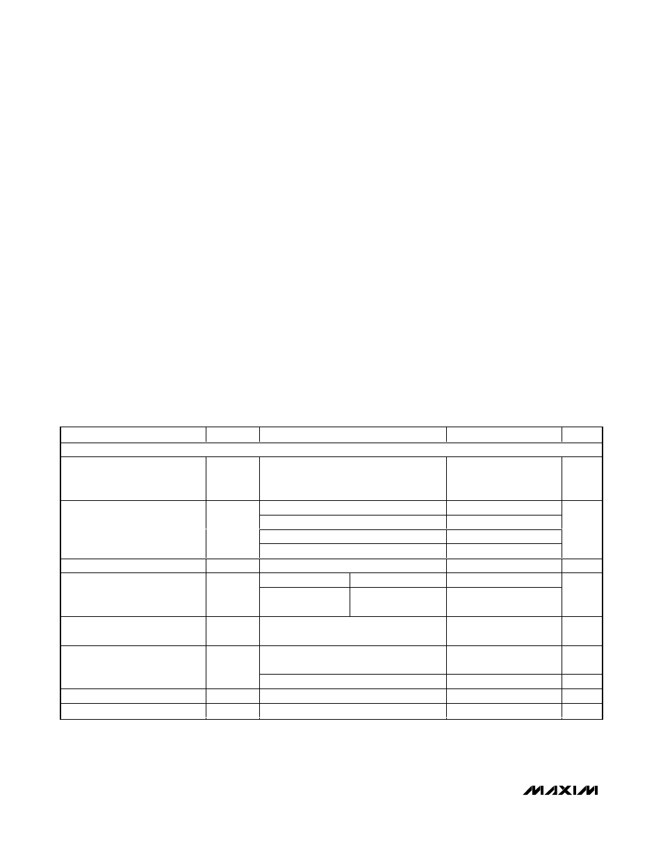
ABSOLUTE MAXIMUM RATINGS
ELECTRICAL CHARACTERISTICS
(V
DD
= PV
DD
= CPV
DD
= 3.3V, GND = PGND = CPGND = 0V, SHDN = V
DD
, I
2
C settings (INA gain = +20dB, INB gain = INC gain =
0dB, volume setting = 0dB, mono path gain = 0dB, SHDN = 1, SSM = 1). Speaker load resistors (R
LSP
) are terminated between
OUT+ and OUT-, headphone load resistors are terminated to GND, unless otherwise noted. C1 = C2 = C3 = 1µF. T
A
= T
MIN
to T
MAX
,
unless otherwise noted. Typical values are at T
A
= +25°C.) (Note 1)
Stresses beyond those listed under “Absolute Maximum Ratings” may cause permanent damage to the device. These are stress ratings only, and functional
operation of the device at these or any other conditions beyond those indicated in the operational sections of the specifications is not implied. Exposure to
absolute maximum rating conditions for extended periods may affect device reliability.
V
DD
to GND ...........................................................................+6V
PV
DD
to PGND .......................................................................+6V
CPV
DD
to CPGND..................................................................+6V
CPV
SS
to CPGND .....................................................-6V to +0.3V
V
SS
to CPGND..........................................................-6V to +0.3V
C1N .......................................(CPV
SS
- 0.3V) to (CPGND + 0.3V)
C1P.......................................(CPGND - 0.3V) to (CPV
DD
+ 0.3V)
HPL, HPR to GND...................(CPV
SS
- 0.3V) to (CPV
DD
+ 0.3V)
GND to PGND and CPGND................................................±0.3V
V
DD
to PV
DD
and CPV
DD
....................................................±0.3V
SDA, SCL to GND.....................................................-0.3V to +6V
All other pins to GND..................................-0.3V to (V
DD
+ 0.3V)
Continuous Current In/Out of PV
DD
, PGND, CPV
DD
, CPGND,
OUT_ _, HPR, and HPL................................................±800mA
Continuous Input Current CPV
SS
....................................+260mA
Continuous Input Current (all other pins) .........................±20mA
Duration of Short Circuit Between
OUT+ and OUT-......................................................Continuous
Duration of HP_ OUT_ Short Circuit to
GND or PV
DD
..........................................................Continuous
Continuous Power Dissipation (T
A
= +70°C)
36-Bump (3mm x 3mm) UCSP Multilayer Board
(derate 17.0mW/°C above +70°C) ...........................1360.5mW
Junction Temperature ......................................................+150°C
Operating Temperature Range ...........................-40°C to +85°C
Storage Temperature Range .............................-65°C to +150°C
Lead Temperature (soldering, 10s) .................................+300°C
PARAMETER
SYMBOL
CONDITIONS
MIN
TYP
MAX
UNITS
GENERAL
Supply Voltage Range
V
DD
,
PV
DD
,
CPV
DD
Inferred from PSRR test
2.7
5.5
V
Output mode 1, 6, 11 (Rx mode)
6.3
10
Output mode 4, 9, 14 (HP mode)
8
12.6
Output mode 2, 7, 12 (SP mode)
11.8
17.5
Quiescent Current
I
DD
Output mode 3, 8, 13 (SP and HP modes)
15.1
21
mA
Mute Current
I
MUTE
Current in mute
4.7
10
mA
Hard shutdown
SHDN = GND
0.1
10
Shutdown Current
I
SHDN
Soft shutdown
See the I
2
C Interface
section
8.5
15
µA
Turn-On Time
t
ON
Time from shutdown or power-on to full
operation
30
ms
B and C pair inputs, T
A
= +25°C,
VOL = max
17.5
28
41.0
k
Ω
Input Resistance
R
IN
A pair inputs, T
A
= +25°C, +20dB
3.5
5.5
8.0
k
Ω
Common-Mode Rejection Ratio
CMRR
T
A
= +25°C, V
IN
= ±500mV
45
50
dB
Input DC Bias Voltage
V
BIAS
IN_ inputs
1.12
1.25
1.38
V