Max9796, Table 2. control registers – Rainbow Electronics MAX9796 User Manual
Page 20
MAX9796
Early STOP Conditions
The MAX9796 recognizes a STOP condition at any point
during data transmission except if the STOP condition
occurs in the same high pulse as a START condition.
Slave Address
The MAX9796 is available with one preset slave
address (see Table 1). The address is defined as the
seven most significant bits (MSBs) followed by the
read/write (R/W) bit. The address is the first byte of
information sent to the MAX9796 after the START condi-
tion. The MAX9796 is a slave device only capable of
being written to. The R/W bit should be a zero when
configuring the MAX9796.
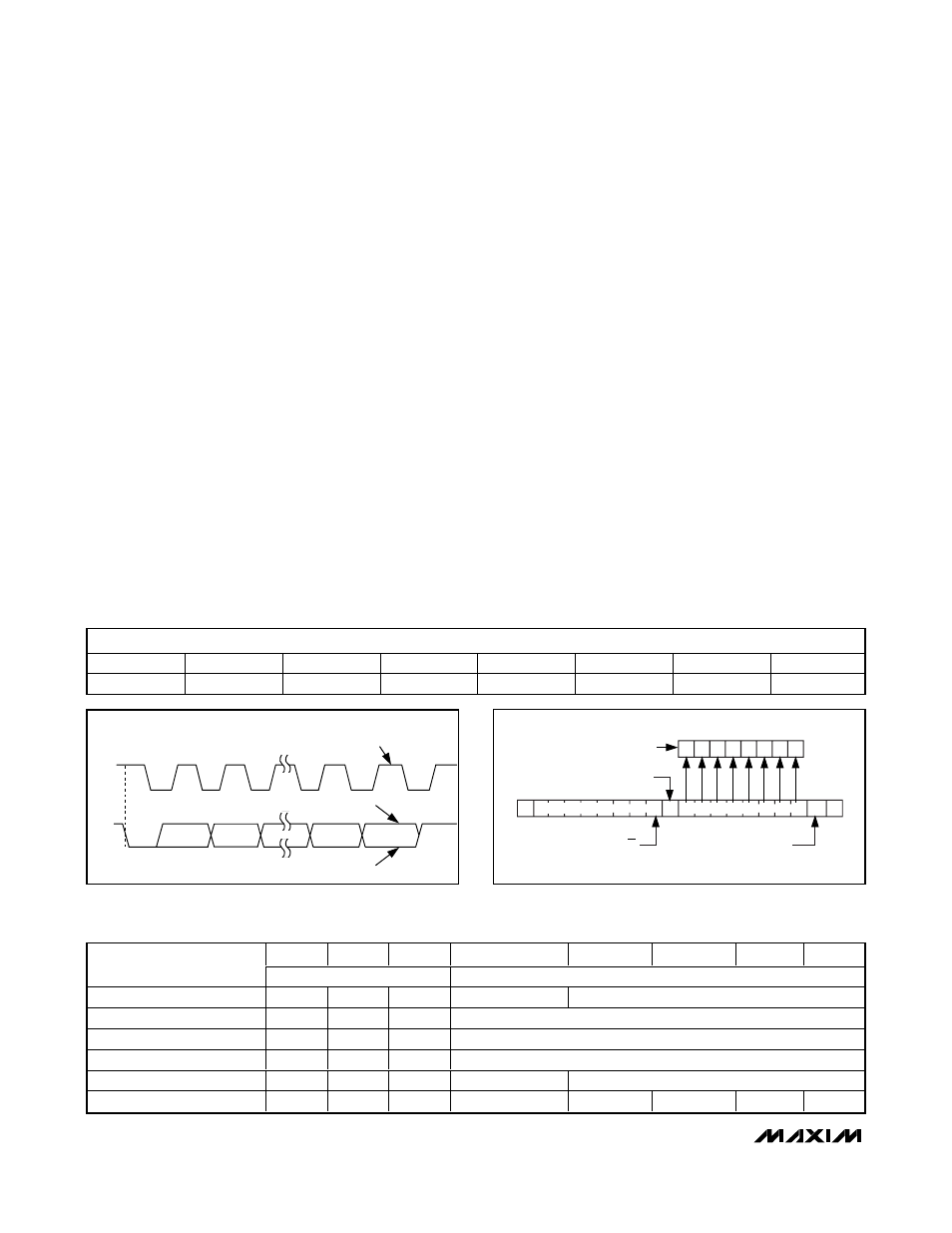
Acknowledge
The acknowledge bit (ACK) is a clocked 9
th
bit that the
MAX9796 uses to handshake receipt of each byte of
data (see Figure 9). The MAX9796 pulls down SDA dur-
ing the master-generated 9
th
clock pulse. Monitoring
ACK allows for detection of unsuccessful data transfers.
An unsuccessful data transfer occurs if a receiving
device is busy or if a system fault has occurred. In the
event of an unsuccessful data transfer, the bus master
may reattempt communications.
Write Data Format
A write to the MAX9796 includes transmission of a
START condition, the slave address with the R/W bit set
to 0 (Table 1), one byte of data to configure the
Command Register, and a STOP condition. Figure 10
illustrates the proper format for one frame.
The MAX9796 only accepts write data, but it acknowl-
edges the receipt of the address byte with the R/W bit
set high. The MAX9796 does not write to the SDA bus
in the event that the R/W bit is set high. Subsequently,
the master reads all 1’s from the MAX9796. Always set
the R/W bit to zero to avoid this situation.
Programming the MAX9796
The MAX9796 is programmed through six control regis-
ters. Each register is addressed by the three MSBs
(B5–B7) followed by five configure bits (B0–B4) as
shown in Table 2. Correct programming of the MAX9796
requires writing to all six control registers. Upon power-
on, their default settings are as listed in Table 3.
2.3W, High-Power Class D Audio Subsystem
with DirectDrive Headphone Amplifiers
20
______________________________________________________________________________________
1
SCL
START
CONDITION
SDA
2
8
9
CLOCK PULSE FOR
ACKNOWLEDGMENT
ACKNOWLEDGE
NOT ACKNOWLEDGE
SLAVE ADDRESS
A6
A5
A4
A3
A2
A1
A0
R/
W
1
0
0
1
1
0
1
0
Figure 9. Acknowledge
S
ACK
0
ACKNOWLEDGE FROM MAX9796
R/W
ACKNOWLEDGE
FROM MAX9796
B7 B6 B5 B4 B3 B2
COMMAND BYTE IS STORED ON
RECEIPT OF STOP CONDITION
ACK
P
B1 B0
SLAVE ADDRESS
COMMAND BYTE
Figure 10. Write Data Format Example
Table 1. MAX9796 Address Map
B7
B6
B5
B4
B3
B2
B1
B0
FUNCTION
COMMAND
DATA
Input Mode Control
0
0
0
INA+20dB
INMODE (Tables 5a and 5b)
Mono Volume Control
0
0
1
MVOL (Table 7)
Left Volume Control
0
1
0
LVOL (Table 7)
Right Volume Control
0
1
1
RVOL (Table 7)
Output Mode Control
1
0
0
MONO+6dB
OUTMODE (Table 9)
Global Control Register
1
0
1
SHDN
IN+6dB
MUTE
SSM
MONO
Table 2. Control Registers