Detailed description, Pin description, Functional diagram – Rainbow Electronics MAX7044 User Manual
Page 6: Typical operating characteristics (continued)
Detailed Description
The MAX7044 is a highly integrated ASK transmitter
operating over the 300MHz to 450MHz frequency
band. The IC requires only a few external components
to complete a transmit solution. The MAX7044 includes
a complete PLL and a highly efficient power amplifier.
The device is automatically placed into a low-power
shutdown mode and powers up when data is detected
on the data input.
Shutdown Mode
The MAX7044 has an automatic shutdown mode that
places the device in low-power mode if the DATA input
has not toggled for a specific amount of time (wait time).
The wait time is equal to 2
16
clock cycles of the crystal.
This equates to a wait time of approximately 6.66ms for
MAX7044
300MHz to 450MHz High-Efficiency,
Crystal-Based +13dBm ASK Transmitter
6
_______________________________________________________________________________________
Pin Description
PIN
NAME
FUNCTION
1
XTAL1
1st Crystal Input. f
XTAL
= f
RF
/ 32.
2
GND
Ground. Connect to system ground.
3
PAGND
Ground for the Power Amplifier (PA). Connect to system ground.
4
PAOUT
Power-Amplifier Output. The PA output requires a pullup inductor to the supply voltage, which can be
part of the output-matching network to an antenna.
5
CLKOUT
Buffered Clock Output. The frequency of CLKOUT is f
XTAL
/ 16.
6
DATA
OOK Data Input. DATA also controls the power-up state (see the Shutdown Mode section).
7
V
DD
Supply Voltage. Bypass to GND with a 100nF capacitor as close to the pin as possible.
8
XTAL2
2nd Crystal Input. f
XTAL
= f
RF
/ 32.
MAX7044
CLKOUT
PAGND
PAOUT
GND
DATA
XTAL1
/16
DATA
ACTIVITY
DETECTOR
LOCK DETECT
32x PLL
PA
CRYSTAL-
OSCILLATOR
DRIVER
XTAL2
V
DD
Functional Diagram
-55
-52
-46
-49
-43
-40
2.1
2.7
2.4
3.0
3.3
3.6
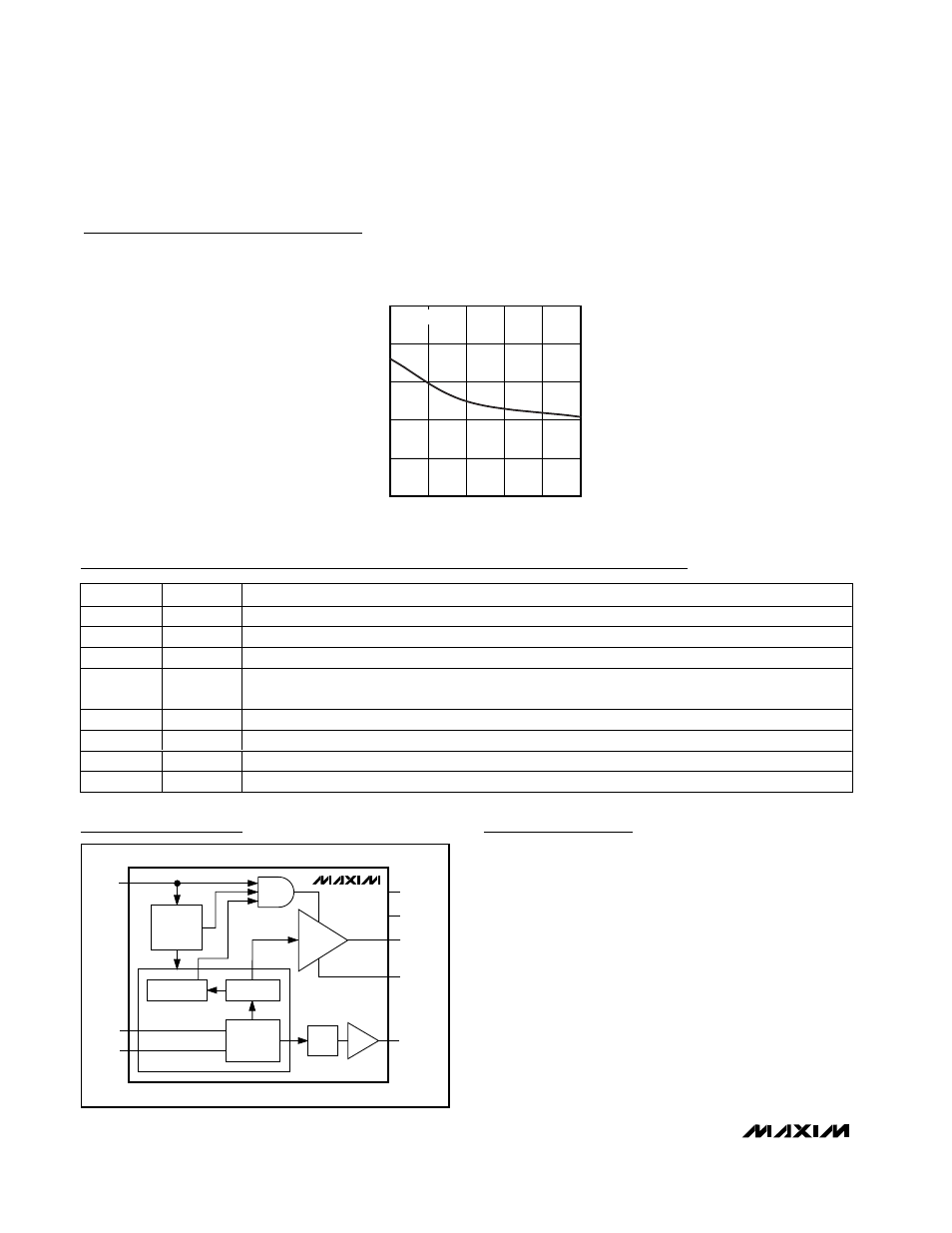
CLKOUT SPUR MAGNITUDE
vs. SUPPLY VOLTAGE
MAX7044 toc19
SUPPLY VOLTAGE (V)
CLKOUT SPUR MAGNITUDE (dBc)
f
RF
= 315MHz
Typical Operating Characteristics (continued)
(Typical Application Circuit, V
DD
= +2.7V, T
A
= +25°C, unless otherwise noted.) (Note 1)