Rainbow Electronics MAX5295 User Manual
Page 9
MAX5290–MAX5295
Buffered, Fast-Settling, Dual, 12-/10-/8-Bit,
Voltage-Output DACs
_______________________________________________________________________________________
9
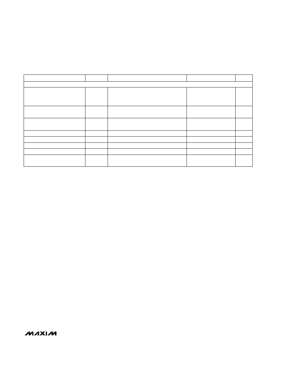
TIMING CHARACTERISTICS—DSP Mode Enabled (1.8V Logic) (Figure 2) (continued)
(DVDD = 1.8V to 3.6V, DGND = 0, TA = TMIN to TMAX, unless otherwise noted.)
PARAMETER
SYMBOL
CONDITIONS
MIN
TYP
MAX
UNITS
UPIO_ TIMING CHARACTERISTICS
DOUT Tri-State Time when
Exiting DOUTDC0, DOUTDC1, or
DOUTRB UPIO_ Modes
t
DOZ
C
L
= 20pF, from end of write cycle to UPIO_
in high impedance
200
ns
DOUTRB Tri-State Time from CS
Rise
t
DRBZ
C
L
= 20pF, from rising edge of CS to UPIO_
in high impedance
40
ns
DOUTRB Tri-State Enable Time
from 8th SCLK Fall
t
ZEN
C
L
= 20pF, from 8th falling edge of SCLK to
UPIO_ driven out of tri-state
40
ns
LDAC Pulse-Width Low
t
LDL
Figure 5
40
ns
LDAC Effective Delay
t
LDS
Figure 6
200
ns
CLR, MID, SET Pulse-Width Low
t
CMS
Figure 5
40
ns
GPO Output Settling Time
t
GP
Figure 6
200
ns
GPO Output High-Impedance
Time
t
GPZ
200
ns
Note 1: For the force-sense versions, FB_ is connected to its respective OUT_. VOUT(max) = VREF / 2, unless otherwise noted.
Note 2: Linearity guaranteed from decimal code 82 to 4095 for the MAX5290B/MAX5291B (12-bit, B-grade), code 21 to 1023 for the
MAX5292/MAX5293 (10-bit), and code 5 to 255 for the MAX5294/MAX5295 (8-bit).
Note 3: DAC-to-DAC crosstalk is measured as follows: outputs of DACA and DACB are set to full scale and the output of DACB is
measured. While keeping DACB unchanged, the output of DACA is transitioned to zero scale and the
∆VOUT of DACB is
measured. The procedure is repeated with DACA and DACB interchanged. DAC-to-DAC crosstalk is the maximum
∆VOUT
measured.
Note 4: Represents the functional range. The linearity is guaranteed at VREF = 2.5V. See the Typical Operating Characteristics sec-
tion for linearity at other voltages.
Note 5: Guaranteed by design.
Note 6: The reference -3dB bandwidth is measured with a 0.1VP-P sine wave on VREF and with the input code at full scale.
Note 7: In some daisy-chain modes, data is required to be clocked in on one clock edge and the shifted data clocked out on the fol-
lowing edge. In the case of a 1/2 clock-period delay, it is necessary to increase the minimum high/low clock times to 25ns
(2.7V) or 50ns (1.8V).
Note 8: The falling edge of DSP starts a DSP-type bus cycle, provided that CS is also active low to select the device. DSP active low
and CS active low must overlap by a minimum of 10ns (2.7V) or 20ns (1.8V). CS can be permanently low in this mode of
operation.