Rainbow Electronics MAX5295 User Manual
Page 2
MAX5290–MAX5295
Buffered, Fast-Settling, Dual, 12-/10-/8-Bit,
Voltage-Output DACs
2
_______________________________________________________________________________________
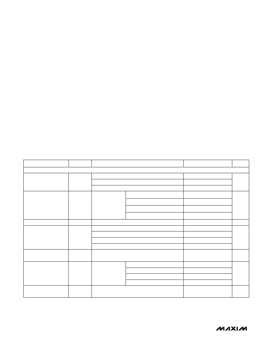
ABSOLUTE MAXIMUM RATINGS
ELECTRICAL CHARACTERISTICS
(AV
DD
= 2.7V to 3.6V, DV
DD
= 1.8V to AV
DD
, AGND = 0, DGND = 0, V
REF
= 2.5V, R
L
= 10k
Ω, C
L
= 100pF, T
A
= T
MIN
to T
MAX
, unless
otherwise noted. Typical values are at T
A
= +25
°C.) (Note 1)
Stresses beyond those listed under “Absolute Maximum Ratings” may cause permanent damage to the device. These are stress ratings only, and functional
operation of the device at these or any other conditions beyond those indicated in the operational sections of the specifications is not implied. Exposure to
absolute maximum rating conditions for extended periods may affect device reliability.
AV
DD
to DV
DD
........................................................................±6V
AGND to DGND ..................................................................±0.3V
AV
DD
to AGND, DGND.............................................-0.3V to +6V
DV
DD
to AGND, DGND ............................................-0.3V to +6V
FB_, OUT_,
REF to AGND ........-0.3V to the lower of (AV
DD
+ 0.3V) or +6V
SCLK, DIN, CS, PU,
DSP to DGND .......-0.3V to the lower of (DV
DD
+ 0.3V) or +6V
UPIO1, UPIO2
to DGND ...............-0.3V to the lower of (DV
DD
+ 0.3V) or +6V
Maximum Current into Any Pin .........................................±50mA
Continuous Power Dissipation (T
A
= +70
°C)
14-Pin TSSOP (derate 9.1mW/
°C above +70°C) .........727mW
16-Pin TSSOP (derate 9.4mW/
°C above +70°C) .........755mW
16-Pin Thin QFN (derate 16.9mW/
°C above +70°C) .1349mW
Operating Temperature Range ...........................-40
°C to +85°C
Storage Temperature Range .............................-65
°C to +150°C
Maximum Junction Temperature .....................................+150
°C
Lead Temperature (soldering, 10s) .................................+300
°C
PARAMETER
SYMBOL
CONDITIONS
MIN
TYP
MAX
UNITS
STATIC ACCURACY
MAX5290/MAX5291
12
MAX5292/MAX5293
10
Resolution
N
MAX5294/MAX5295
8
Bits
MAX5290A/MAX5291A (12-bit)
±1
MAX5290B/MAX5291B (12-bit)
±2
±4
MAX5292/MAX5293 (10-bit)
±0.5
±1
Integral Nonlinearity
INL
V
REF
= 2.5V at
AV
DD
= 2.7V
(Note 2)
MAX5294/MAX5295 (8-bit)
±0.125
±0.5
LSB
Differential Nonlinearity
DNL
Guaranteed monotonic (Note 2)
±1
LSB
MAX5290A/MAX5291A (12-bit), decimal code = 40
±5
MAX5290B/MAX5291B (12-bit), decimal code = 82
±5
±25
MAX5292/MAX5293 (10-bit), decimal code = 21
±5
±25
Offset Error
V
OS
MAX5294/MAX5295 (8-bit), decimal code = 5
±5
±25
mV
Offset-Error Drift
5
ppm of
FS/
°C
MAX5290A/MAX5291A (12-bit)
±4
MAX5290B/MAX5291B (12-bit)
±10
±20
MAX5292/MAX5293 (10-bit)
±3
±5
Gain Error
GE
Full-scale output
MAX5294/MAX5295 (8-bit)
±0.5
±2
LSB
Gain-Error Drift
1
ppm of
FS/
°C