Table 23. gpi read command, Table 24. unipolar code table (gain = +1) – Rainbow Electronics MAX5295 User Manual
Page 27
MAX5290–MAX5295
Buffered, Fast-Settling, Dual, 12-/10-/8-Bit,
Voltage-Output DACs
______________________________________________________________________________________
27
GPI, GPOL, GPOH
UPIO1 and UPIO2 can each be configured as a gener-
al-purpose logic input (GPI), a general-purpose logic-
low output (GPOL), or general-purpose logic-high
output (GPOH).
The GPI can detect interrupts from µPs or microcon-
trollers. It provides three functions:
1) Sample the signal at GPI at the time of the read
(RTP1 and RTP2).
2) Detect whether or not a falling edge has occurred
since the last read or reset (LF1 and LF2).
3) Detect whether or not a rising edge has occurred
since the last read or reset (LR1 and LR2).
RTP1, LF1, and LR1 represent the data read from
UPIO1. RTP2, LF2, and LR2 represent the data read
from UPIO2.
To issue a read command for the UPIO configured as
GPI, use the command in Table 23.
Once the command is issued, RTP1 and RTP2 provide
the real-time status (0 or 1) of the inputs at UPIO1 or
UPIO2, respectively, at the time of the read. If LF2 or
LF1 is one, then a falling edge has occurred on the
UPIO1 or UPIO2 input since the last read or reset. If
LR2 or LR1 is one, then a rising edge has occurred
since the last read or reset.
GPOL outputs a constant logic low, and GPOH outputs
a constant logic high (see Figure 6).
TOGG
Use the TOGG input to toggle a DAC output between
the values in the input register and DAC register. A
delay of greater than 100ns from the end of the previ-
ous write command is required before the TOGG signal
can be correctly switched between the new value and
the previously stored value. When TOGG = 0, the out-
put follows the information in the input registers. When
TOGG = 1, the output follows the information in the
DAC register (Figure 5).
FAST
The MAX5290–MAX5295 have two settling-time-mode
options: FAST (3µs max at 12 bits) and SLOW (6µs max
at 12 bits). To select the FAST mode, drive FAST low,
and to select SLOW mode, drive FAST high. This over-
rides (not overwrites) the SPDA and SPDB bit settings.
Table 23. GPI Read Command
DATA
CONTROL BITS
DATA BITS
DIN
1
1
1
1
0
0
1
X
X
X
X
X
X
X
X
X
DOUTRB
X
X
X
X
X
X
X
X
X
X
RTP2
LF2
LR2
RTP1
LF1
LR1
Table 24. Unipolar Code Table (Gain = +1)
DAC CONTENTS
MSB
LSB
ANALOG OUTPUT
1111
1111
1111
+V
REF
(4095 / 4096)
1000
0000
0001
+V
REF
(2049 / 4096)
1000
0000
0000
+V
REF
(2048 / 4096) = V
REF
/ 2
0111
1111
1111
+V
REF
(2047 / 4096)
0000
0000
0001
+V
REF
(1 / 4096)
0000
0000
0000
0
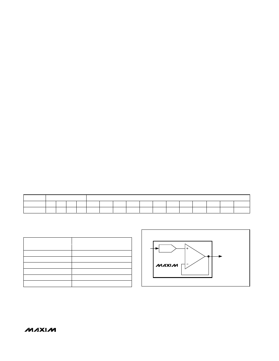
MAX5290
DAC_
REF
OUT_
V
OUT_
= V
REF
x CODE / 4096
CODE IS THE DAC_ INPUT
CODE (0 TO 4095 DECIMAL).
Figure 7. Unipolar Output Circuit
X = Don’t care.