Serial-interface programming commands, Loading input and dac registers – Rainbow Electronics MAX5295 User Manual
Page 17
MAX5290–MAX5295
Buffered, Fast-Settling, Dual, 12-/10-/8-Bit,
Voltage-Output DACs
______________________________________________________________________________________
17
SCLK
DIN
C3
C2
C1
C0
D11
D10
D9
D8
D7
D6
D5
D4
D3
D2
D1
D0
DIN
SCLK
DV
DD
COMMAND TAKES EFFECT HERE
ONLY IF SCLK COUNT = N
✕
16
COMMAND TAKES EFFECT HERE
ONLY IF SCLK COUNT = N
✕
16
MICROWIRE OR SPI (CPOL = 0, CPHA = 0) 8-BIT CONTROL DATA OR 12-BIT DAC DATA WRITE:
CS MUST REMAIN LOW BETWEEN BYTES ON A 16-BIT WRITE OPERATION
SPI (CPOL = 1, CPHA = 1) 8-BIT CONTROL DATA OR 12-BIT DAC DATA WRITE:
CS MUST REMAIN LOW BETWEEN BYTES ON A 16-BIT WRITE OPERATION
DIN
SCLK
CS
CS
MAX5290–
MAX5295
V
DD
V
DD
MICROWIRE
SK
SO
I/O
SCLK
DIN
DV
DD
MAX5290–
MAX5295
V
DD
V
DD
SPI OR QSPI
SCK
MOSI
SS OR I/O
CS
DSP
DSP
CS
C3
C2
C1
C0
D11
D10
D9
D8
D7
D6
D5
D4
D3
D2
D1
D0
SCLK
DIN
C3
C2
C1
C0
D11
D10
D9
D8
D7
D6
D5
D4
D3
D2
D1
D0
C3
C2
C1
C0
D11
D10
D9
D8
D7
D6
D5
D4
D3
D2
D1
D0
DIN
SCLK
DGND
COMMAND TAKES EFFECT HERE
ONLY IF SCLK COUNT = N
✕
16
COMMAND TAKES EFFECT HERE
ONLY IF SCLK COUNT = N
✕
16
DSP OR SPI (CPOL = 0, CPHA = 0) 8-BIT CONTROL DATA OR 12-BIT DAC DATA WRITE:
DSP OR SPI (CPOL = 1, CPHA = 0) 8-BIT CONTROL DATA OR 12-BIT DAC DATA WRITE:
DIN
SCLK
CS
CS
MAX5290–
MAX5295
V
SS
DSP
TCLK, SCLK, OR CLKX
DT OR DX
TFS OR FSX
SCLK
DIN
DGND
MAX5290–
MAX5295
V
SS
SPI OR QSPI
SCK
MOSI
SS OR I/O
CS
DSP
DSP
CS
CS MUST REMAIN LOW BETWEEN BYTES ON A 16-BIT WRITE OPERATION
CS MUST REMAIN LOW BETWEEN BYTES ON A 16-BIT WRITE OPERATION
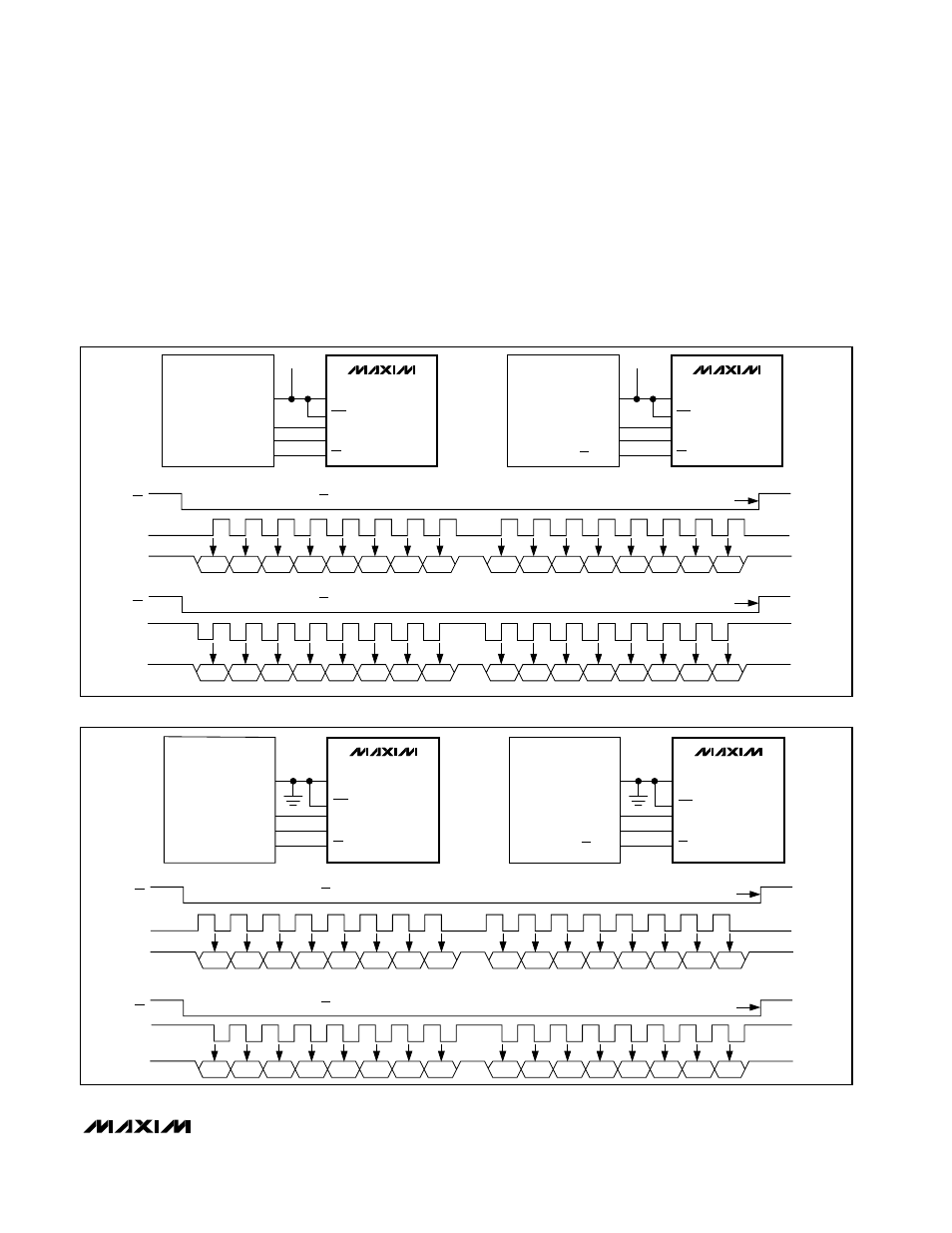
Figure 3. MICROWIRE and SPI (CPOL = 0, CPHA = 0 or CPOL = 1, CPHA = 1) DAC Writes
Figure 4. DSP and SPI (CPOL = 0, CPHA = 1 or CPOL = 1, CPHA = 0) DAC Writes
Serial-Interface Programming Commands
Tables 2a, 2b, and 2c provide all of the serial-interface
programming commands for the MAX5290–MAX5295.
Table 2a shows the basic DAC programming com-
mands, Table 2b gives the advanced-feature program-
ming commands, and Table 2c provides the 24-bit
read commands. Figures 3 and 4 illustrate the serial-
interface diagrams for read and write operations.
Loading Input and DAC Registers
The MAX5290–MAX5295 contain a 16-bit shift register
that is followed by a 12-bit input register and a 12-bit
DAC register for each channel (see the Functional
Diagrams). Tables 3, 4, and 5 highlight a few of the com-
mands for the loading of the input and DAC registers.
See Table 2a for all DAC programming commands.