Power-supply and layout considerations – Rainbow Electronics MAX5295 User Manual
Page 29
MAX5290–MAX5295
Buffered, Fast-Settling, Dual, 12-/10-/8-Bit,
Voltage-Output DACs
______________________________________________________________________________________
29
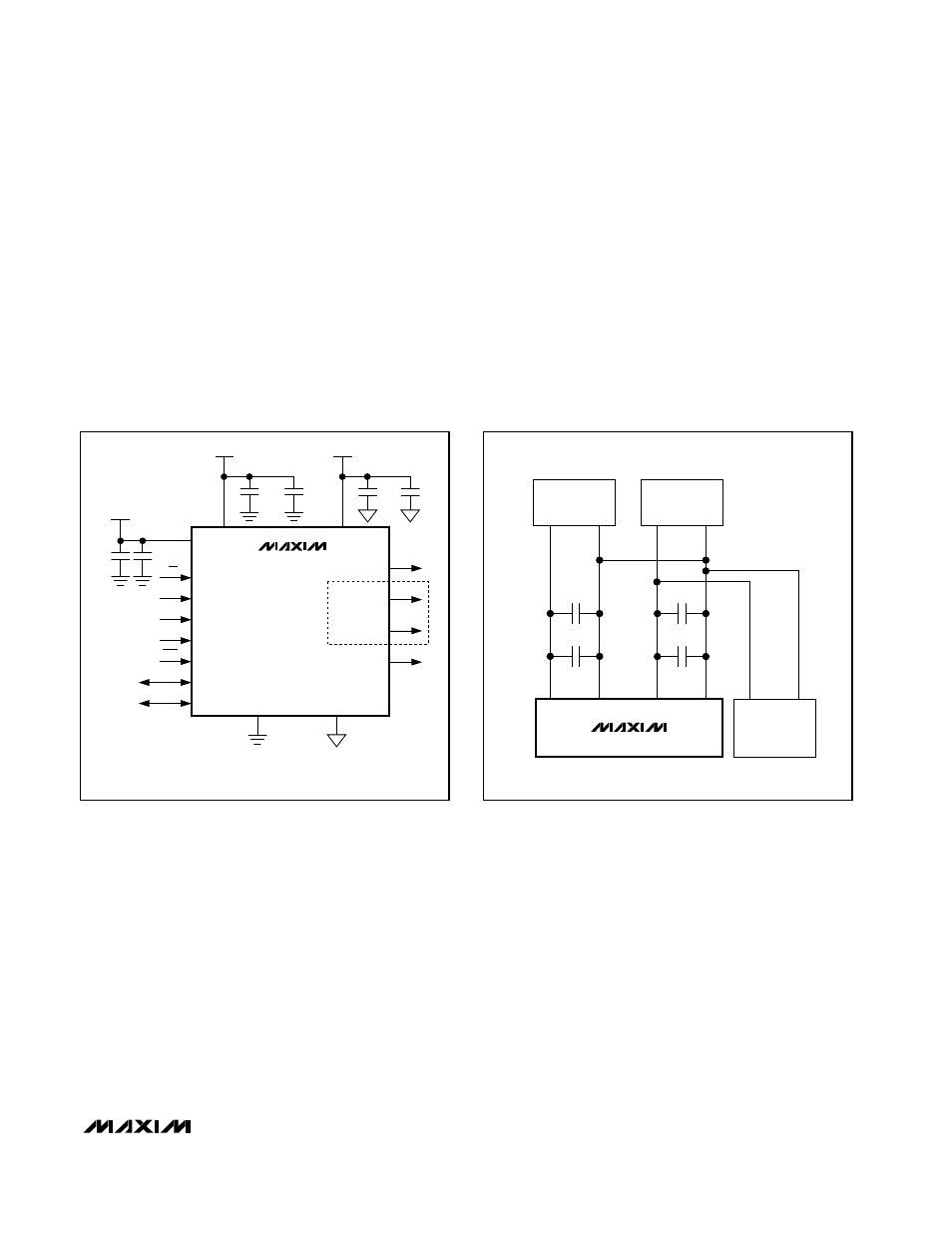
Power-Supply and Layout Considerations
Bypass the analog and digital power supplies with a
10µF capacitor in parallel with a 0.1µF capacitor to ana-
log ground (AGND) and digital ground (DGND) (see
Figure 10). Minimize lead lengths to reduce lead induc-
tance. If noise is an issue, use shielding and/or ferrite
beads to increase isolation.
Digital and AC transient signals coupling to AGND cre-
ate noise at the output. Connect AGND to the highest
quality ground available. Use proper grounding tech-
niques, such as a multilayer board with a low-induc-
tance ground plane. Wire-wrapped boards and sockets
are not recommended. For optimum system perfor-
mance, use printed circuit (PC) boards with separate
analog and digital ground planes. Connect the two
ground planes together at the low-impedance power-
supply source.
Using separate power supplies for AV
DD
and DV
DD
improves noise immunity. Connect AGND and DGND at
the low-impedance power-supply source (see Figure 11).
MAX5290–MAX5295
V
REF
10
µF*
0.1
µF*
REF
SCLK
DIN
PU
UPIO1
UPIO2
CS
DSP
AGND**
DGND**
OUTA
FBA
FBB
OUTB
MAX5291/
MAX5293/
MAX5295
ONLY
10
µF
0.1
µF
0.1
µF
10
µF
DV
DD
AV
DD
DV
DD
AV
DD
*REMOVE BYPASS CAPACITORS ON REF FOR AC-REFERENCE INPUTS.
**CONNECT ANALOG AND DIGITAL GROUND PLANES AT THE
LOW-IMPEDANCE POWER-SUPPLY SOURCE.
Figure 10. Bypassing Power Supplies and Reference
MAX5290–MAX5295
0.1
µF
10
µF
AV
DD
AGND
AV
DD
AGND
0.1
µF
10
µF
DV
DD
DGND
DV
DD
DGND
DV
DD
DGND
ANALOG SUPPLY
DIGITAL SUPPLY
DIGITAL
CIRCUITRY
Figure 11. Separate Analog and Digital Power Supplies