Table 13. settling-time-mode write example, Table 14. settling-time-mode read command, Table 17. cpol and cpha read command – Rainbow Electronics MAX5295 User Manual
Page 23: Table 15. cpol and cpha bits, Table 16. cpol and cpha write command
MAX5290–MAX5295
Buffered, Fast-Settling, Dual, 12-/10-/8-Bit,
Voltage-Output DACs
______________________________________________________________________________________
23
Settling-Time-Mode Bits (SPDA, SPDB)
The settling-time-mode bits select the settling time
(FAST mode or SLOW mode) of the MAX5290–
MAX5295. Set SPD_ = 1 to select FAST mode or set
SPD_ = 0 to select SLOW mode, where “_” is replaced
by A or B, depending on the selected channel (see
Table 12). FAST mode provides a 3µs maximum set-
tling time and SLOW mode provides a 10µs maximum
settling time. Default settling-time mode bits are [0, 0]
(SLOW mode for both DACs).
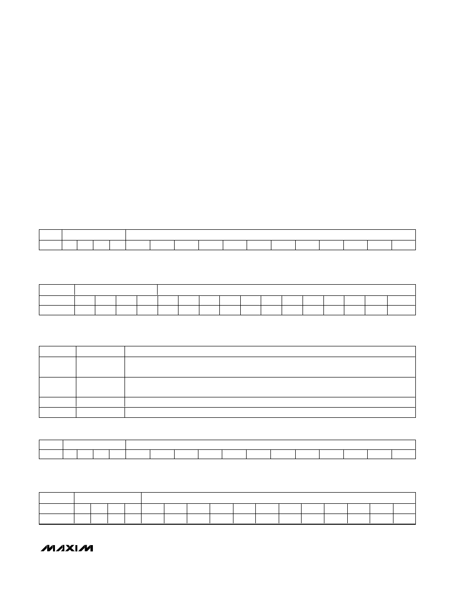
Settling-Time-Mode Write Example:
To configure DACA into FAST mode and DACB into
SLOW mode, use the command in Table 13.
To read back the settling-time-mode bits, use the com-
mand in Table 14.
CPOL and CPHA Control Bits
The CPOL and CPHA control bits of the
MAX5290–MAX5295 are defined the same as the CPOL
and CPHA bits in the SPI standard. Set the CPOL = 0
and CPHA = 0 or set CPOL = 1 and CPHA = 1 for
MICROWIRE and SPI applications requiring the clocking
of data in on the rising edge of SCLK. Set the CPOL = 0
Table 13. Settling-Time-Mode Write Example
DATA
CONTROL BITS
DATA BITS
DIN
1
1
1
0
1
1
0
X
X
X
X
X
X
X
0
1
X = Don’t care.
Table 14. Settling-Time-Mode Read Command
DATA
CONTROL BITS
DATA BITS
DIN
1
1
1
0
1
1
1
X
X
X
X
X
X
X
X
X
DOUTRB
X
X
X
X
X
X
X
X
X
X
X
X
X
X
SPDB
SPDA
Table 17. CPOL and CPHA Read Command
DATA
CONTROL BITS
DATA BITS
DIN
1
1
1
1
0
0
0
1
X
X
X
X
X
X
X
X
DOUTRB
X
X
X
X
X
X
X
X
X
X
X
X
X
X
CPOL
CPHA
Table 15. CPOL and CPHA Bits
CPOL
CPHA
DESCRIPTION
0
0
Default values at power-up when DSP is connected to DV
DD
. Data is clocked in on the rising edge
of SCLK.
0
1
Default values at power-up when DSP is connected to DGND. Data is clocked in on the falling edge
of SCLK.
1
0
Data is clocked in on the falling edge of SCLK.
1
1
Data is clocked in on the rising edge of SCLK.
Table 16. CPOL and CPHA Write Command
DATA
CONTROL BITS
DATA BITS
DIN
1
1
1
1
0
0
0
0
X
X
X
X
X
X
CPOL
CPHA
X = Don’t care.
X = Don’t care.
X = Don’t care.