Pin description – Rainbow Electronics MAX5295 User Manual
Page 12
MAX5290–MAX5295
Buffered, Fast-Settling, Dual, 12-/10-/8-Bit,
Voltage-Output DACs
12
______________________________________________________________________________________
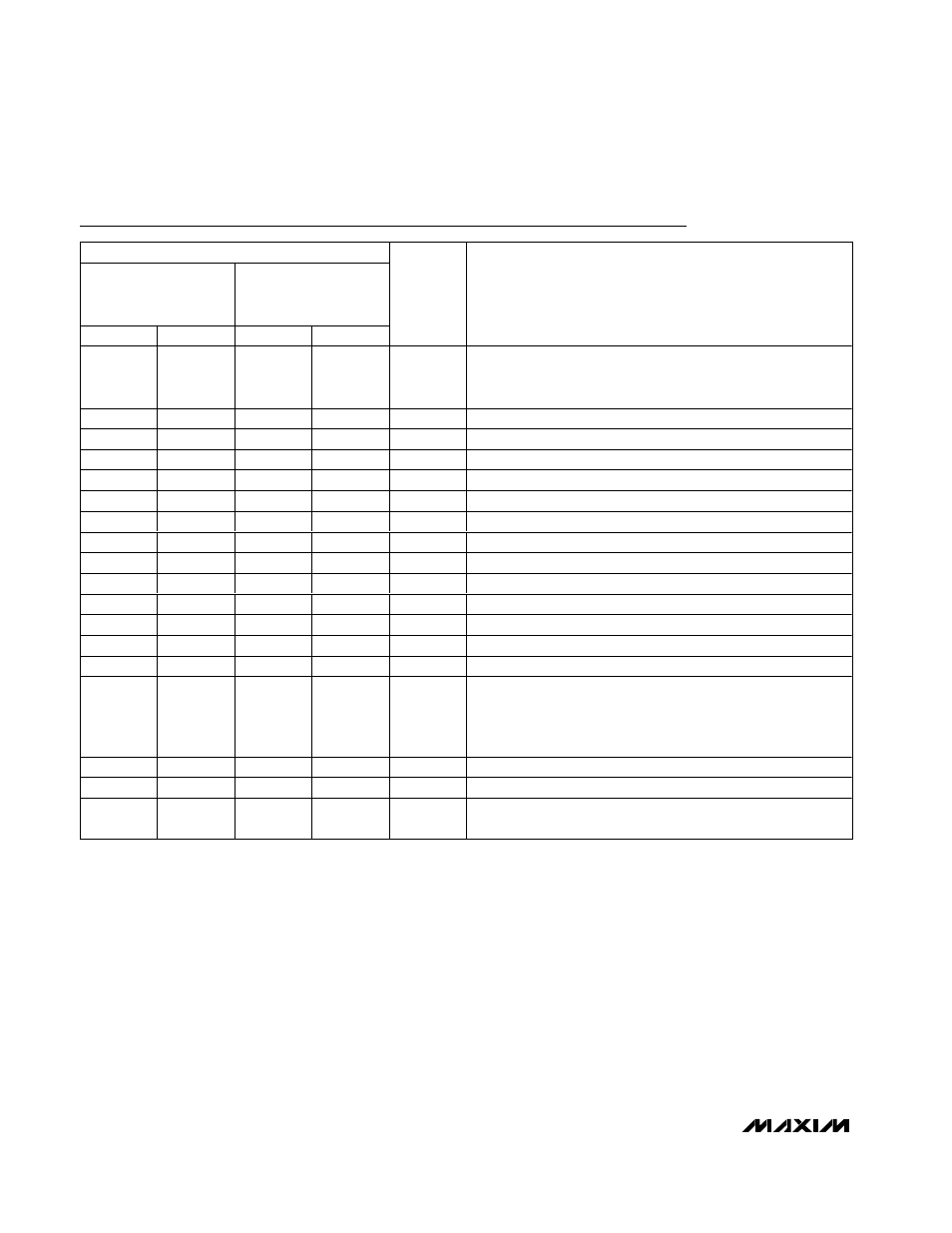
Pin Description
PIN
MAX5290
MAX5292
MAX5294
MAX5291
MAX5293
MAX5295
THIN QFN
TSSOP
THIN QFN
TSSOP
NAME
FUNCTION
1
2
1
3
DSP
Clock Enable. Connect DSP to DV
DD
at power-up to transfer
data on the rising edge of SCLK. Connect DSP to DGND at
power-up to transfer data on the falling edge of SCLK.
2
3
2
4
DIN
Serial Data Input
3
4
3
5
CS
Active-Low Chip-Select Input
4
5
4
6
SCLK
Serial Clock Input
5
6
5
7
DV
DD
Digital Supply
6
7
6
8
DGND
Digital Ground
7
8
7
9
AGND
Analog Ground
8
9
8
10
AV
DD
Analog Supply
9
10
9
11
OUTB
DACB Output
—
—
10
12
FBB
Feedback for DACB Output Buffer
10
11
11
13
REF
Reference Input
—
—
12
14
FBA
Feedback for DACA Output Buffer
11, 13
—
—
—
N.C.
No Connection. Not internally connected.
12
12
13
15
OUTA
DACA Output
14
13
14
16
PU
Power-Up State Select Input. Connect PU to DV
DD
to set OUTA
and OUTB to full scale upon power-up. Connect PU to DGND to
set OUTA and OUTB to zero upon power-up. Leave PU floating
to set OUTA and OUTB to midscale upon power-up.
15
14
15
1
UPIO2
User-Programmable Input/Output 2
16
1
16
2
UPIO1
User-Programmable Input/Output 1
—
—
—
—
EP
Exposed Paddle (QFN Only). Not internally connected. Do not
connect to circuitry.