Rainbow Electronics MAX5295 User Manual
Page 6
MAX5290–MAX5295
Buffered, Fast-Settling, Dual, 12-/10-/8-Bit,
Voltage-Output DACs
6
_______________________________________________________________________________________
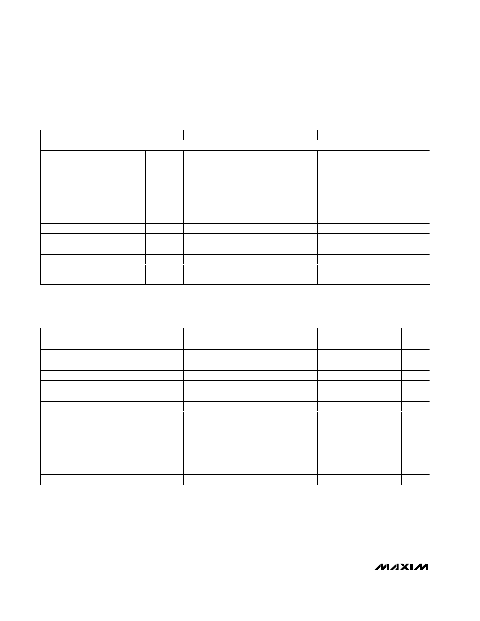
TIMING CHARACTERISTICS—DSP Mode Disabled (3V, 3.3V Logic) (Figure 1) (continued)
(DVDD = 2.7V to 3.6V, DGND = 0, TA = TMIN to TMAX, unless otherwise noted.)
PARAMETER
SYMBOL
CONDITIONS
MIN
TYP
MAX
UNITS
UPIO TIMING CHARACTERISTICS
DOUT Tri-State Time when Exiting
DOUTDC0, DOUTDC1, or
DOUTRB UPIO Modes
t
DOZ
C
L
= 20pF, from end of write cycle to UPIO_
in high impedance
100
ns
DOUTRB Tri-State Time from CS
Rise
t
DRBZ
C
L
= 20pF, from rising edge of CS to UPIO_
in high impedance
20
ns
DOUTRB Tri-State Enable Time
from 8th SCLK Rise
t
ZEN
C
L
= 20pF, from 8th rising edge of SCLK to
UPIO_ driven out of tri-state
20
ns
LDAC Pulse-Width Low
t
LDL
Figure 5
20
ns
LDAC Effective Delay
t
LDS
Figure 6
100
ns
CLR, MID, SET Pulse-Width Low
t
CMS
Figure 5
20
ns
GPO Output Settling Time
t
GP
Figure 6
100
ns
GPO Output High-Impedance
Time
t
GPZ
100
ns
TIMING CHARACTERISTICS—DSP Mode Disabled (1.8V Logic) (Figure 1)
(DVDD = 1.8V to 3.6V, DGND = 0, TA = TMIN to TMAX, unless otherwise noted.)
PARAMETER
SYMBOL
CONDITIONS
MIN
TYP
MAX
UNITS
SCLK Frequency
f
SCLK
1.8V < DV
DD
< 3.6V
10
MHz
SCLK Pulse-Width High
t
CH
(Note 7)
40
ns
SCLK Pulse-Width Low
t
CL
(Note 7)
40
ns
CS Fall to SCLK Rise Setup Time
t
CSS
20
ns
SCLK Rise to CS Rise Hold Time
t
CSH
0
ns
SCLK Rise to CS Fall Setup Time
t
CS0
10
ns
DIN to SCLK Rise Setup Time
t
DS
20
ns
DIN to SCLK Rise Hold Time
t
DH
5
ns
SCLK Rise to DOUTDC1 Valid
Propagation Delay
t
DO1
C
L
= 20pF, UPIO_ = DOUTDC1 mode
60
ns
SCLK Fall to DOUT_ Valid
Propagation Delay
t
DO2
C
L
= 20pF, UPIO_ = DOUTDC0 or DOUTRB
mode
60
ns
CS Rise to SCLK Rise Hold Time
t
CS1
MICROWIRE and SPI modes 0 and 3
20
ns
CS Pulse-Width High
t
CSW
90
ns