Electrical characteristics (continued) – Rainbow Electronics MAX5295 User Manual
Page 3
MAX5290–MAX5295
Buffered, Fast-Settling, Dual, 12-/10-/8-Bit,
Voltage-Output DACs
_______________________________________________________________________________________
3
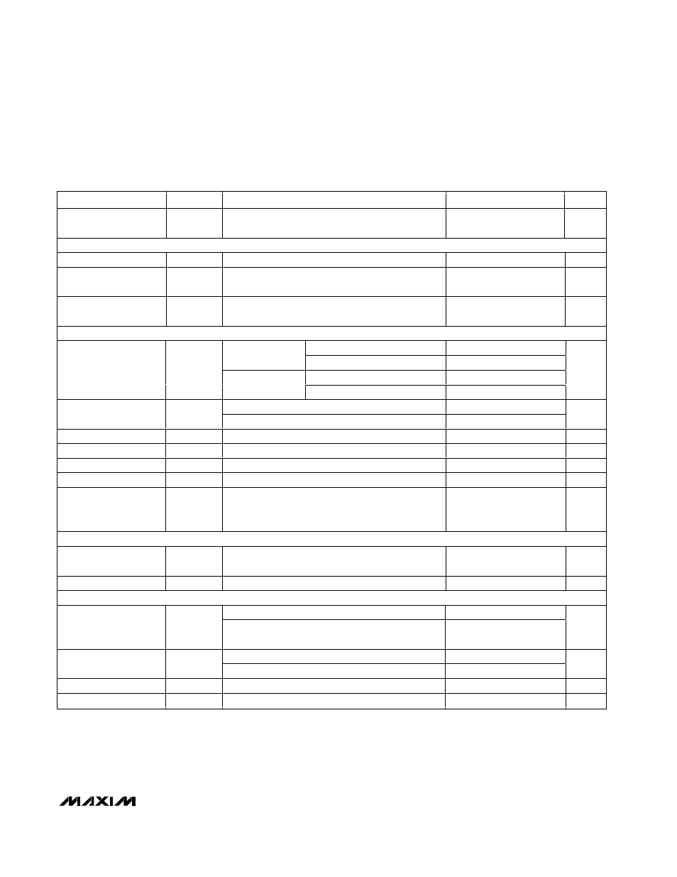
ELECTRICAL CHARACTERISTICS (continued)
(AV
DD
= 2.7V to 3.6V, DV
DD
= 1.8V to AV
DD
, AGND = 0, DGND = 0, V
REF
= 2.5V, R
L
= 10k
Ω, C
L
= 100pF, T
A
= T
MIN
to T
MAX
, unless
otherwise noted. Typical values are at T
A
= +25
°C.) (Note 1)
PARAMETER
SYMBOL
CONDITIONS
MIN
TYP
MAX
UNITS
Power-Supply Rejection
Ratio
PSRR
Full-scale output, AV
DD
= 2.7V to 3.6V
200
µV/V
REFERENCE INPUT
Reference Input Range
V
REF
0.25
AV
DD
V
Reference Input
Resistance
R
REF
Normal operation (no code dependence)
145
200
k
Ω
Reference Leakage
Current
I
REF
Shutdown mode
0.5
1
µA
DAC OUTPUT CHARACTERISTICS
Unity gain
85
SLOW mode,
full scale
Force sense
67
Unity gain
140
Output Voltage Noise
FAST mode,
full scale
Force sense
110
µV
RMS
Unity-gain output
0
AV
DD
Output Voltage Range
(Note 4)
Force-sense output
0
AV
DD
/ 2
V
DC Output Impedance
38
Ω
Short-Circuit Current
AV
DD
= 3V, OUT_ to AGND, full scale, FAST mode
45
mA
Power-Up Time
From DV
DD
applied, interface is functional
30
60
µs
Wake-Up Time
Coming out of shutdown, outputs settled
40
µs
Output OUT_ and FB_
Open-Circuit Leakage
Current
Programmed in shutdown mode, force-sense
outputs only
0.01
µA
DIGITAL OUTPUTS (UPIO_)
Output High Voltage
V
OH
I
SOURCE
= 2mA
DV
DD
-
0.5
V
Output Low Voltage
V
OL
I
SINK
= 2mA
0.4
V
DIGITAL INPUTS (SCLK, CS, DIN, DSP, UPIO_)
2.7V
≤ DV
DD
≤ 3.6V
2.4
Input High Voltage
V
IH
DV
DD
< 2.7V
0.7 x
DV
DD
V
2.7V
≤ DV
DD
≤ 3.6V
0.6
Input Low Voltage
V
IL
DV
DD
< 2.7V
0.2
V
Input Leakage Current
I
IN
±0.1
±1
µA
Input Capacitance
C
IN
10
pF