Rainbow Electronics MAX5128 User Manual
Page 9

Digital Interface
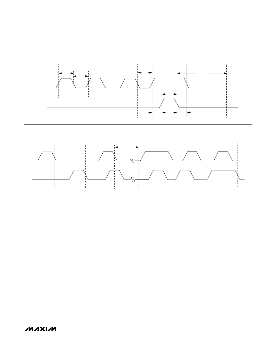
The MAX5128 features a 2-wire interface consisting of
two logic inputs (UP and DN). Logic inputs UP and DN
control the wiper position and program the position to
the nonvolatile memory. Transition UP from high to low
with DN low to increment the wiper position. Transition
DN from high to low with UP low to decrement the wiper
position (see Figures 1, 2, and 3). When the wiper decre-
ments, it decreases the resistance between W and L
(and it increases the resistance between H and W).
To program the nonvolatile memory, force UP high,
then force DN high, and then transition either input
(UP/DN) from high to low (see Figure 3).
The wiper performs a make-before-break transition,
ensuring that an open circuit during a transition from
one resistor tap to another does not occur. The wiper
does not wrap around when it reaches either end of the
resistor array (max/min). Additional transition com-
mands in the direction of the end point do not change
the tap position.
The logic inputs also feature pulse glitch immunity
(20ns) to protect the wiper from transitioning due to
glitches (see Figure 4).
When using the MAX5128 with a momentary contact
switch, use the MAX6817 to debounce the logic inputs
(UP/DN) (see Figure 5).
Write NV Register
The internal EEPROM consists of a 7-bit nonvolatile
memory that retains the value written to it even after
power-down. To program the nonvolatile memory, force
UP high, then force DN high, and then transition either
input (UP/DN) from high to low. A nonvolatile write
requires a busy time of 14ms (max). During the busy
time, any nonvolatile write requests are ignored as well
as requests to increment or decrement the wiper posi-
tion. Upon power-up, the wiper returns to the position
stored in the nonvolatile register. The MAX5128 fea-
tures a factory-default wiper position of midscale.
MAX5128
128-Tap, Nonvolatile, Linear-Taper Digital
Potentiometer in 2mm x 2mm µDFN Package
_______________________________________________________________________________________
9
t
PWH
t
PWL
t
MS2
t
BUSY
UP
DN
t
WS
t
WH
t
WP
NVM
WRITE
Figure 2. Digital-Interface Timing Diagram with t
BUSY
WIPER
INCREMENTS
NVM
WRITE
UP
DN
t
BUSY
WIPER
DECREMENTS
NVM
WRITE
WIPER
INCREMENTS
WIPER
DECREMENTS
Figure 3. Digital-Interface Command Diagram
